Showing posts with label a. Show all posts

Saturday, December 21, 2013

Build a Inexpensive Isolation Transformer Circuit Diagram

Build a Inexpensive Isolation Transformer Impromptus Setup Circuit Diagram. Using two 12-V filament or power transformers, an impromptu isolation transformer can be made for low-power (under 50 W) use in testing or servicing. SOI is an ordinary, duplex ac recept-able. Use heavy-wire connections between the 12-V windings because several amperes can flow.

Inexpensive Isolation Transformer Circuit Diagram


Inexpensive Isolation Transformer Circuit Diagram

ReadMore..

Thursday, October 10, 2013

Short Circuit Protection With A MOSFET

If you have an application in which a MOSFET is already used to switch a load, it is relatively easy to add short-circuit or overload protection. Here we make use of the internal resistance RDS(ON), which produces a voltage drop that depends on the amount of current flowing through the MOSFET. The voltage across the internal resistance can be sensed using simple comparator or even a transistor, which switches on at a voltage of around 0.5V. You can thus avoid the use of a sense resistor (shunt), which usually produces an undesirable extra voltage drop. The comparator can be monitored by a microcontroller. In case of an overload, the software can initiate suitable countermeasures (PWM regulation, alarm, emergency stop etc.). It is also conceivable to connect the comparator output directly to the gate of the MOSFET, in order to immediately cut off the transistor in case of a short circuit.

Short-Circuit Protection With A MOSFET Circuit Diagram
ReadMore..

Monday, October 7, 2013

14W CLASS A AMPLIFIER USING 2N3055 ELECTRONIC DIAGRAM

14W CLASS A AMPLIFIER USING 2N3055 ELECTRONIC DIAGRAM

Why Class A ? Because , when biased to class A, the transistors are always turned on, always ready to respond instantaneously to an input signal. Class B and Class AB output stages require a microsecond or more to turn on. The Class A operation permits cleaner operation under the high-current slewing conditions that occur when transient audio signal are fed difficult loads. His amplifier is basically simple, as can be seen from the block diagram.
ReadMore..

Sunday, September 1, 2013

A Basic IR Link

Description:
A basic Imfra Red Link for audio communication for distances upto 3 metres.


Notes:
Ovo je shema jednostavne bez?i?ne komunikacije sa malo komponenata .Diode d1 i d2 su infracrvene le-diode ,a foto transistor je tako?er infracrveni radi ?to manjeg vanjskog utjecaja .Domet ure?aja je oko 3m no on se mo?e promijeniti brojem le-dioda i naponom koji se dovede na diode.Na izlaz se ?ak mogu i direktno spojiti slu?alice.Link mo?e poslu?iti i za prijenos drugih vrsta signala..Na popisu komponenata nema kriti?nih dijelova i izrada sklopa je jako jeftina. Uz malo pa?nje ne moe da ne radi.
P.S Transistors can be replaced with 2N3904 and 2N2222

Notes:
In his circuit Milan has created a basic Infra Red transmitter and receiver. The transmitter comprises a single amplifying stage driving two series connected IR LEDS. The input source is connected to J1. Please note that the device will pass a small DC current through it and also directly bias the transistor. A suitable device is therefore a high output crystal microphone. These can produce high output voltages up to 1 Volt but this will be reduced by the transistors low input impedance.

The receiver is three stages, the first stage being a phototransistor. Stages two and three form a high gain darlington emitter follower, the bias for the whole stage derived through R2 and the phototransistor itself. C1 and R3 form a filter to reduce interference from flourescent lighting and other hum sources. The output is via Jack J2. Note also that the output device will pass a small DC current so a medium impedance loudspeaker or hwadphones are a good choice here.
ReadMore..

Sunday, August 4, 2013

Build a LT3582 12 DC 5V to 12V DC Converter

Using LT3582-12 dual channel DC DC converter integrated circuit, manufactured by Linear Technology, can be designed a very simple step up dc converter. This 5 to 12V c converter electronic project provide both positive and negative outputs required in many biasing applications such as active matrix OLED (organic light-emitting diode)displays as well as CCD (charge coupled device) applications.

Build a LT3582-12 DC 5V to 12V DC Converter

The LT3582 offer an I2C interface that can dynamically program output voltages, power sequencing and output voltage ramps as the application requires. The LT3582’s positive output voltage can be set between 3.2V and 12.775 in 25mV steps, whereas the negative output can be set between -1.2V and -13.95V in 50mV steps. The LT3582-12 is preconfigured with ±12V output, requiring no future programming.
ReadMore..

Thursday, July 11, 2013

Build a 35W Bridge Power Amplifier with TDA2030

This is the schematic diagram of 35W bridge power amplifier circuit, delivers 35W power output for 8? speaker. The circuit is similar to this 15W bridge amplifier. It use two pieces of amplifier IC TDA2030 (you may use LM1875 as subtitute/replacement).

 Build a 35W Bridge Power Amplifier with TDA2030

Build a 35W Bridge Power Amplifier with TDA2030


Notes:
  • Use 15V/3A power supply for maximum performance.
  • Use heatsink to prevent overheating on the IC
Parts List:
R1,3,5,7,9 = 22K?
R2,8 = 680?
R4,6 = 1?
C1 = 4.7uF/16V
C2,7 = 22uF/16V
C3,6 = 220nF
C4,9 = 100nF
C5,8 = 200uF/25V
IC1-2 = TDA2030 / LM1875
Lsp = 8?/ 60W Loudspeaker


ReadMore..

Saturday, July 6, 2013

Build a MHz Oscillator using an ATtiny15

Most engineers will recognise the problem: Your circuit needs a stable 1 or 2 MHz clock generator (in the author’s case it was for a Pong game using an old AY3-8500). A suitable crystal is not to hand so you cobble together an RC oscillator (there are plenty of circuits for such a design). Now it turns out that you don’t have exactly the right capacitor so a preset pot is add e d to allow some adjustment . Before you know it the clock circuit is taking up more space on the board than you had hoped. 

Providing the application does not demand a precise clock source a tiny 8-pin microcontroller may offer a better solution to the problem. It needs no additional external components and an old ATtiny15 can be found quite cheaply. Another advantage of the solution is that clock frequency adjustment does not involve changing external components and is not subject to component tolerances. 

The microcontroller’s internal RC oscillator is already accurately calibrated to 1.6 MHz. With its inbuilt PLL, internal Timer 1 can achieve up to 25.6 MHz [2]. By configuring internal dividers the timer can output a frequency in range of roughly 50 kHz up to 12 MHz from an output pin. The difference between calculated and the actual output frequency increases at higher frequencies. A meaningful upper limit of about 2 MHz is a practical value and even at this frequency the deviation from the calculated value is about 15 %.

MHz Oscillator using an ATtiny15 Schematic

MHz Oscillator using an ATtiny15 Circuit Diagram
The circuit diagram could hardly be simpler, aside from the power supply connections the output signal on pin 6 (PB1) is the only other connection necessary.The example program, written in Assembler is just 15 lines long! With a program this short comments are almost super fluous but are included for clarity. The code can be downloaded from the Elektor website [1]. 

The program only needs to initialise the timer which then runs independently of processor control to output the clock sign al . The processor can then be put into sleep mode to memory used up the remaining 99 % is free for use for other tasks if required. 

The OSCCAL register contains a calibration byte which allows some adjustment of the CPU clock. This gives a certain degree of fine tuning of the output frequency. A recommendation in the Atmel data sheet indicates that the CPU clock frequency should not be greater than 1.75 MHz otherwise timer operation cannot be guaranteed. 

The more recent ATtiny45 can be substituted for the ATtiny15. In this case the CK SEL fuses should be set to put the chip’s Timer 1 into ATtiny15- compatible mode [3]. After adjustment to the program it will now be possible to obtain a higher (or more exact) frequency from the timer, the ATtiny45’s PLL can operate up to 64 MHz. Link
ReadMore..

Friday, April 12, 2013

How to Make a Simple Timer Circuit Using IC 555


A timer is a device which produces a delay period after which an external connected electrical load is triggered. The produced time delay is normally adjustable and the user has the freedom to set the time period as desired. There are many ways of making simple timer circuits using different ICs and discrete components; here we discuss one such circuit using the ubiquitous IC 555.


The IC 555 is a pretty common electronic part among the electronic enthusiasts and is also very popular due to the involved simple configurations and low component count.

The two popular multivibrator modes of operation that’s associated with this IC are the astable mode, and the monostable mode. Both of these are useful configurations and have plenty of different applications.

For the present design we incorporate the second mode of operation, which is the monostable mode.

In this mode of operation the IC is configured to receive a trigger externally, so that it’s output changes state, meaning if with reference to the ground if the output of the IC is zero, then it would become positive as soon as the trigger (momentary) is received at its input terminal.

This change in its output is sustained for a certain period if time, depending upon the external time determining components. Normally the time determining components are in the form of a resistor and a capacitor which together determine or fix the time period for which the IC output would hold its “high” position.

By changing either the value of the capacitor or the resistor, the timing can be altered as desired. The above time fixing components are termed as the RC component.

The figure shows a very straightforward design where the IC 555 forms the central controlling part of the circuit. As discussed in the above section, the IC is in its standard monostable mode.

Pin #2 receives the external timing trigger from a push-to-ON switch. Once this switch is pushed, the circuit pulls its output to a positive potential   and holds it until the predetermined time delay lapses.

The entire circuit can be built over a small piece of general PCB and housed inside a neat looking plastic enclosure along with the battery.

The output may be ideally connected to a buzzer for receiving the warning alarm after the set time lapses.

Parts List

R1, R4 = 4K7,
R2 = 10K,
R3 = 1M pot,
C1 = 0.47uF,
C2 = 1000uF/25V,
C3 = 0.01uF,
IC1 = 555,
Bz1 = Piezo Buzzer,
Push Button = push to ON switch

A circuit design requested by Mr.Bourgeoisie:


ReadMore..

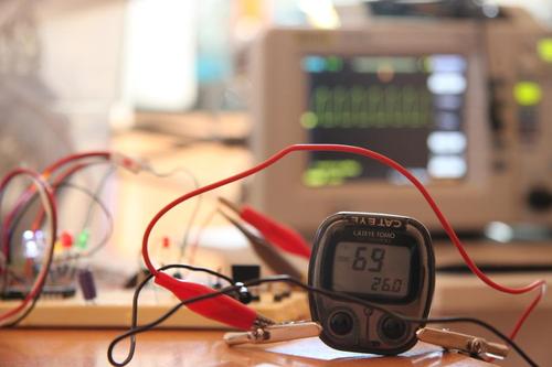
Track Your Distance Through a Bicycle Odometer

Just like cars that measures the distance it can travel, you can also do it with your bicycles. We usually keep track of our mileage to see how far our strength can go but would it be of great use if we track it because we are maintaining a workout everyday considering the calories we are burning.

Hacks and Mods: Track Your Distance Through a Bicycle Odometer

If you want to make your own odometer, you will need a micro controller that generates pulse and a MOSFET that converts those voltage pulses. Just remember to check your batteries all the time.
The best way of burning calories is to move those muscles everyday! Set your bikes and your odometer! Burn fats!
 
 
Streamcircuits
ReadMore..

Thursday, April 11, 2013

Building a radio station

Requires us to make things systematically and efficiently, because time is very valuable to us, then some of the advances in technology has been applied in various fields, including education, because this is where all the technological advances developed.Lots of technology is rapidly expanding in our country today. With technology growing by leaps and bounds this is what will make the work more systematic and efficient.Based on our technological advances and his friends create a system are related to the Electronics course, we propose the same faculty to develop a community tool. We got a second job in four semesters, which makes the FM transmitter.
Departing from hobby assembling electronic items, we try to assemble a mini-power transmitter that can emit a short signal of approximately 100 meters with power (power) 5 watts. This is a pilot who later became 12 watts. With 12 watts of power, radio broadcasts to reach a village. 
1.2 Formulation of ProblemProblems are handled from this lab assignment is to create and analyze the quality of an FM transmitter to get the data at test point 1, point 2 test, test point 3 and the exact frequency as desired.Things are of practical tasks is restricted only to analyze the quality of a transmitter and retrieve data from an existing test point. 
1.3 LimitationsProblems to be addressed in this lab assignment is limited to some of the following:1 • Retrieving data from the frequency and calculate TP 1 to TP 3.2 • Analyze a transmitter in the room, based on measurement data and make conclusions. 
1.4 ObjectivesObjectives to be achieved in this task are:A. Students can design and make the circuit in fm transmitter.2. 12 Watt FM transmitter that can be made of appropriate tools and can be marketed. 
1.5 MethodologyIn completing this lab assignment, the steps are as follows:1 • Learn about basic electronics concepts and learn concepts about the mechanism of FM modulation.2 • Analyze and conclude the experimental results, and give advice when it is applied to the practical task of the real system.3 • Preparing a report on second semester practicum assignment. 
1.6 DiscussionThis book of this lab assignment consists of 5 (five) chapters, in each chapter related to one another, namely: 
CHAPTER 1:Provide background on the issues, goals, problems and constraints of the problems discussed in this lab assignment.CHAPTER 2:Provide the theoretical basis to support problem solving in this lab assignment. The basic theory is given include: the mechanism of the tool inused in making the FM transmitter 
CHAPTER 3:Planning and manufacture of tools and how each blog diagram contained in FM transmitterCHAPTER 4:Contains the results of calculations and data processing, and analysis resultscalculation.CHAPTER 5:Provide conclusions about the results already obtained and suggestions.CHAPTER IIBASIC THEORY 
2.1 Koker

Koker serves to regulate or determine the frequency of the radio transmitter. In koker also Ferrite that serves as a core inductor in addition there is an inductance coil comprising primary and secondary winding. Way of working is to facilitate search koker empty wave. When filling koker in turn to the right to a maximum frequency of the oscillator produce more low. If the FM transmitter lights, turn left up the core koker to hissing on the FM radio signal is lost it will be found a strong and stable.

2.2 Inductor

Coil of wire that is wrapped with a particular matter, in this case to determine the value of the inductor is typically used Q-meter. Inductor serves as an impedance adjustment, so that the output of the impedance can be changed and in accordance with the desired (match).


2.3 Transistor

 Transistors have two connections, one of which is the emitter and the other base and collector. Because this is a transistor as two diodes. ransistor C1970 type normally used to raise the voltage 0.8 to 1 watt, I think it was in the C1970 study could increase about 8 times.On the C1971 transistor can be coupled directly from the exciter circuit and the voltage of 6.5 to 7 watts or bias raised about 10 times.If the C1970 to C1971 join the output power of about 12 watts or more. (All will be explained in Chapter III) 

2.4 ExciterExciter circuit consists of an oscillator and buffer.•  OscillatorTransmitter is the core of an oscillator. To be able to build a good communication system should begin with an oscillator that can work perfectly. In the communication system, the oscillator generates a sine wave is used as the carrier signal. Then the information signal is superimposed on a carrier signal with the modulation process.•  Buffer (Buffer)All types of oscillators require a buffer. Buffer serves to stabilize the frequency and / or amplitude of the oscillator from loading the next level. Usually a buffer consisting of 1 or 2 levels of the transistor amplifier dibias as class A.The heart of the broadcast transmitter FM exciter is located on it. Function of the exciter is to generate and modulate a carrier wave with one or more input (mono, stereo, SCA) in accordance with FCC standards. Which has been modulated carrier wave is then amplified by a wideband amplifier to the level required by the next level. 

2.5 BoosterPower amplifier is more popularly known as Booster. Booster is a device mounted radio transmitters attached to and used to amplify radio frequency transmit power in any direction that you want to go. For example, for a transmitter power of 25 watts which include only a single village, Booster is used to transmit power to be 50 to 100 watts so it can besurrounding the district. Boosters are generally small squares connected by cable to the transmitter which he built.Power amplifier is divided into two. First, the power amplifier which amplifies the signal in one cycle, the best signal quality and harmonious. The second, which only reinforces the power amplifier input signal is less than half of the cycle and generate a wave that damaged the same frequency.


2.6 Antenna

 Antenna function and simultaneously capture signals radiate radio wave radiation. The antenna is divided into two by the beam, ie• omnidirectional (all directions). This antenna radiates radio waves are equally strong all directions.• Bidirectional (both directions). This antenna radiates equally strong radio waves to only two directions. Two parameters that need to be considered is the polarization of the antenna and its gain. Put simply, an antenna has vertical polarization if the antenna is placed in a position perpendicular to the earth. Antenna with vertical polarization would produce radio waves with vertical polarization as well. In addition to the vertical, some horizontal polarized antenna, when the antenna is positioned parallel to the field of the earth.

2.7 Transmission LineTransmission line is the introduction to the generated power to the transmitter antenna. As an introduction to power, a good transmission line will not reduce the power of delivery and did not radiate, because it is the duty antennas radiate. So that the maximum power transfer occurs, then the transmission line characteristic impedance should also have the same view of resource load. Transmission line characteristic impedance is 300 W common (ribbon cable to the black and white TV), 75 W (on a color TV coaxial cable) and 50W (coaxial cable to the amateur radio equipment).Additional tools are in need in assembling a 12-watt FM transmitter, among which are:
 •  Power MeterPower Meter is a tool to measure the wave. On a transmission line that is not worth it, but the waves come rolling waves are reflected. Wave dating from the source to the load direction (from transmitter to antenna), while the reflected wave from the opposite direction (from the antenna to the transmitter). Usually on the Power Meter has two scales, onecame to power and one for the reflected power. The reflected power scale to be smaller than the scale for the future.
 •  SWR MeterSWR meter or measuring comparative standing waves are used to measure the ratio of the incident wave and reflected wave. So it is known how a resource commensurate with the burden. The working principle is based on the Power Meter SWR Meter. If there is only one Power Meter measurements, the SWR can be calculated from the incident power (Pf) andthe reflected power (Pr) with the formula:SWR = (OPF + ÖPr) (OPF - ÖPr).
• From the formula, the state equivalent (Pr = O) will be obtained SWR = 1.
• For a state that is not worth going to get SWR> 1.
• For the worst circumstances in which all power is reflected back dating (Pf = Pr) will get the SWR = infinity.
•  Dummy LoadTo be able to broadcast a maximum transmit power, but efficient, it takes a load impedance that is known with certainty as it is called Dummy Load reference. Dummy Load is free from the influence of frequency and can handle the disposal of the transmit power is too great. Dummy Load impedance is usually 50 or 75 Ohm. Dummy Load can be made withput some resistors in parallel in order to obtain the desired resistance and power. Parallelize some resistors minimize the stray inductance of the resistor. For example, can use the carbon resistor 300 Ohm / 2 watt for 6 seeds that are connected in parallel to get the Dummy Load with power of 12 watts and 50 Ohm impedance.

CHAPTER IIIPLANNING AND DEVELOPMENT TOOLS
3.1. PreliminaryTo plan and create a 12 Watt FM transmitter, need to know first about a block diagram of the system, the working system of the circuit isOverall, the calculations and planning.
3.2. System Block Diagram and Figure Series Overall

The picture above shows a block diagram of this system and imageThe overall network is made in full.Transmission System Block Diagram picture as a whole
3.2.1 Block diagram of the image transmitter exciter circuit FM

Picture Exciter Circuit Network consists of exciter oscillator and buffer. In this Exciter Network using the specification of components as follows:•  Koker•  Inductor: L2 = 0.12 micro-Henry, Henry Micro L3 = 0.12, L4 = 0.2 micro-Henry•  Transistor: C930•  Ohm: 5.6 K, 47 K, 33 K•  Babysitter WANTED: 2.2 nF, 100 nF, 18 pF, 20 pF, 5 pF•  trimer: 5-60 pFExciter is a network that produces oscillations, because the exciter are oscillator that acts as a sine wave generator and it will be dimodulasikan. In the oscillator system is also available buffer (buffer) that functions to stabilize the frequency / modulation oscillator amplifier due to the loading process by the next level. 
3.2.2 Network Booster (Power Amplifier)

The series of images BoosterIn the Booster circuit uses components withthe following specifications: 
 •  Inductors: L1 = 0.2 micro-Henry. L2 = 0.2 micro-Henry. 0085 L3 = L4 = 0.04 micro micro Henry Henry. L5 = 0.1 micro-Henry. L6 = 0.2 micro-Henry L7 = 0.2 micro-Henry. 
 •  Transistor 1970: 10 V VCEIc 0.1 AΒ 10-180 
 •  trimer: 5-30 pFBooster circuit consists of two levels of transistor amplifiers, each working on a class C, each input and output transistor amplifier circuit is given impedance adjustment.Strengthening of the first transistor using C1970. Strengthening the circuit has a 9.2 dB power gain (8 times), so that from the exciter-power 0.25 W of power generated should be 2 W. In fact the output of this first level of reinforcement produces only 1.75 Watt power, this is due to the loss of matching network circuit.Strengthening of the second level using transistor C1971. The amplifier circuit has a 10dB power gain (10 times). So that the power of the first level of 1.75 W can be strengthened to 17.5 W. In fact strengthening the power of the second level only reached 12.5 Watt. 
This is due to the loss of matching network and the limited range ofC1971 transistor. Because the price of the C1971 transistor is relatively expensive it is to use only the C1970 transistor. Therefore, the power generated by the transmitter is not as high as 12 Watt. Because of the heat generated second transistor is large enough then we put enough cooling. 

CHAPTER IVTESTING TOOLS4.1 
GeneralThis chapter discusses the testing and analysis system that has been made. In general, this test aims to determine if the device has been realized that can be worked in accordance with a predetermined plan specifications. The purpose of the tests performed on the system are as follows: 
•  Knowing how the exciter circuit 
•  Knowing how the booster circuit


4.2 Testing exciter circuit
•  The purposeTo find out if the oscillator can work well and achieve the desired frequency. And also to determine whether the buffer is running properly.
•  The equipment usedA. Koker2. Inductor3. Transistor4. Resistor5. Trimer6. Dummy Load7. 5 volt power supply8. Multimeter9. Frequency Counter10. PCB
•  The test procedureTest Block DiagramA. Assemble the equipment used in accordance Picture2. Provide 12 volt power supply to the exciter circuit3. Switch the exciter circuit to get the most power in large4. Calculate the voltage at TP 1, TP 2 and, TP 35. Observe the output (at V output)
•  The test resultsThe test results are shown in Table. the following:Exciter circuit Testing ResultsTest Results PointA 0.6V2 0.6V3 11.75 V
 4.3 Testing a series of booster
•  The purposeTo gain greater power and also increase the distance range of further emission up to 7-fold.
•  The equipment usedA. Inductor2. Transistor3. Trimer4. Dummy Load5. 12 Volt Power Supply
•  The test procedureTesting Block Diagram Picture Booster:A. Assemble the equipment used in accordance Picture2. Large test circuit voltage that can be accepted3. Observing the output
•  The test resultsThe test results are shown in Table. the following:Booster circuit Testing ResultsTest Results Point4 11,755 11,75

 CHAPTER VCLOSING
5.1. ConclusionBased on the test results it can be concluded:
•  In a series of FM transmitters weve made, the power output is only 2 Watt for C1970 transistor used is that only 1 Watt power up
•  FM transmitter that can be made only reach 93 MHz frequency
•  The distance achieved depends on the power emitted by the FM transmitter
 5.2 Advice
•  If you want to make the transmitter starts with a good oscillator.
• If you want to make a series of FM with a power greater then use the transistor C1971, C1946. the power generated about 25 watts.
• To balance the output of the FM transmitter mounted circuit PLL (Phase Local Loop).


ReadMore..

Friday, April 5, 2013

How to Make a Simple VU Meter Circuit at Home

VU meter or a volume unit meter is a device used for indicating the music volume output from an amplifier or a loudspeaker system. It may be also considered as a device for displaying the PMPO of the amplifier at a particular volume setting.
Though the unit looks quite  technical, which is applied as a measuring device of audio power, in real terms these are more like decorative ornaments of an amplifier. Without such devices attached, an amplifier system would look quite dull and without any juice.
The varying response from a VU meter certainly gives a whole new dimension to a sound system making it more dynamic with its features.
Prior to the days when LEDs were not so popular, moving coil meter type of displays were commonly incorporated as VU meters and surely these units with there back lights ON produced a distinctive visual effect as their needles deflected from left to right displaying the varying pitch of the connected audio system.
With the advent of  the LEDs, the moving coil displays slowly got replaced with the ones which incorporated LEDs.
With color effect at its disposal, LEDs became the HOT favorites as far as VU meter were concerned, even today amplifiers employ a LED VU graph for displaying the music power in an amplifier.
For electronic hobbyists who are rather more interested in building a particular required gagdet right at home instead of buying a commercial piece, this cool VU meter circuit will interest them if they are intending to make one for their music system.
The circuit of a simple LED VU meter explained here uses the outstanding chip LM3915 from TEXAS Instruments.
The circuit diagram shows a very simple configuration employing two of the above ICs in the cascaded form for producing a good 20 LED sequencing bar type indication.
The music input is applied across pin #5 and ground of the IC. The music input can be directly derived from the speaker terminals of the music system.
R3 has been stationed for adjusting the typical dB levels between the LEDs for enabling visually more enhanced sequencing pattern in response to the fed music input.
The diagram shows a separate power supply being used for the circuit, however if the amplifier supports a 12 volt stabilized power supply, can be used for powering the circuit as well, this would help to get rid of the extra bulk involving the transformer and the associated rectification circuitry.
The color of the LEDs may be selected as indicated in the diagram or may be altered as desired by the user.
Everything is pretty straight forward and can be simply built over a general purpose board.
Assemble the IC first and then go on fixing the rest of the components and connect then to the relevant pin outs of the IC.
The LEDs should be soldered at the end, such that all of them are arranged in a straight line, preferably at the edge of the PCB.
An external enclosure may be used for housing the assembled circuit or possibly the circuit may be installed in the amplifier dashboard itself, if situation permits the required drilling and fittings.


ReadMore..