Showing posts with label with. Show all posts

Thursday, October 10, 2013

Short Circuit Protection With A MOSFET

If you have an application in which a MOSFET is already used to switch a load, it is relatively easy to add short-circuit or overload protection. Here we make use of the internal resistance RDS(ON), which produces a voltage drop that depends on the amount of current flowing through the MOSFET. The voltage across the internal resistance can be sensed using simple comparator or even a transistor, which switches on at a voltage of around 0.5V. You can thus avoid the use of a sense resistor (shunt), which usually produces an undesirable extra voltage drop. The comparator can be monitored by a microcontroller. In case of an overload, the software can initiate suitable countermeasures (PWM regulation, alarm, emergency stop etc.). It is also conceivable to connect the comparator output directly to the gate of the MOSFET, in order to immediately cut off the transistor in case of a short circuit.

Short-Circuit Protection With A MOSFET Circuit Diagram
ReadMore..

Monday, September 30, 2013

9V DC Adapter With Battery Backup

With just a low cost DC adapter and the circuit described here it is possible to build a low cost stabilized, uninterruptable 9V supply. On the grounds of safety and economy, a simple unstabilized 12V D.C. adapter is used as the power source, a universal adapter with its output set to 12 V will do equally well. The output voltage of an adapter under low load conditions (up to approximately 1/3 of the rated output current) is over 15 V, even at the rated output current, there will be sufficient voltage to supply a 9 V voltage regulator. The rating of the DC adapter should be chosen according to the output current required at 9V. Common values are 300mA, 500mA and 1A.

The 9V voltage regulator used in this circuit has a built in thermal shutdown mechanism so that if too much current is drawn from the device, it simply turns off as it overheats and will not supply any current until the case temperature returns to normal. If the unit is intended to supply more than say 150-200mA then to prevent thermal shutdown it will be necessary to fit a heatsink to the voltage regulator. The rule of thumb used to calculate the size of heatsink is that you should be able to touch it during operation at maximum load, without burning you finger. When choosing the DC adapter, it is always better to select one with a higher current rating than is needed this will ensure that its output voltage is high enough to be able to also charge the 12V cells.

DC Adapter with Battery Backup Circuit DiagramAs long as mains voltage is on the DC adapter, the voltage across C1 will be higher than the voltage of the cells. Charging current will flow through R1 and D1 to the cells. Current also flows to the voltage regulator and out to the load connected at the output. Diode D2 in this situation will not conduct because the voltage at its cathode is greater than that at its anode When the mains voltage fails or is turned off, diode D2 conducts and current will now flow from the Nickel Cadmium cells to the voltage regulator, thereby automatically keeping the output voltage at 9V. The value of resistor R1 is chosen so that a charging current to the cells is not greater than 1/10th of the cells capacity (if the cells are rated at 1100mAh, the charging current must not exceed 110mA).

From the point of view of cell longevity it is better to reduce this charging current even further (1/20 or 1/50 C). When calculating this resistor, the value of the no-load voltage should be used. This will give the highest charging current. To calculate the charging current using R1 with a value of 180 Ω. The cells measure 13.8 V when fully charged and the no-load output voltage of the DC adapter is 17V. Charging current is given by the formula: (17V – 13.8V – 0.7V) / 180 = 13.9mA. Substituting the actual measured values in this formula will enable you to calculate the value of R1 to give the correct charging current for the cells.
ReadMore..

Sunday, September 29, 2013

Simple Knock Alarm With Piezo Sensor

This circuit uses a thin piezoelectric sensor to sense the vibrations generated by knocking on a surface; eg, a door or table. Basically, it amplifies and processes the signal from the sensor and sounds an alarm for a preset period. In operation, the piezoelectric sensor converts mechanical vibration into an electrical signal. This sensor can be attached to a door, a cash box, cupboard, etc using adhesive. A 1-1.5m long shielded cable can then be connected between the sensor plate and the input of the circuit. The signal generated by the sensor is amplified by transistors Q1-Q3 which are wired as common-emitter amplifiers.

Simple knock alarm with piezo sensor circuit schematic

The signal is then rectified by diode D1 and amplified by transistors Q4-Q6. As shown, the output from Q6s collector is fed to pin 4 (reset) of 555 timer IC1. This is wired as an astable multivibrator. Each time Q6 turns on, its collector goes high and IC1 activates and produces an alarm tone in the speaker. The alarm automatically turns off 10s after knocking ceases - ie, the time taken for the 22µF capacitor on Q4s emitter to discharge. Finally, note that it may be necessary to adjust the 470O resistor in Q6s collector circuit to ensure that IC1 remains off in the absence of any perceptible knock. A value somewhere between 220O and 680O should be suitable.
ReadMore..

Thursday, September 26, 2013

Light Gate With Counter Using 555 And 4033

The circuit described here counts the number of times that an infrared beam is interrupted. It could be used to count the number of people entering a room, for instance, or how often a ball or another object passes through an opening (handy for playing shuffleboard). The heart of the circuit consists of - you guessed it - a light gate! Diode D1 is an IR diode that normally illuminates IR transistor T1. The light falling on T1 causes it to conduct to a certain extent. The resulting voltage on the collector of T1 should be just low enough to prevent the following transistor (T2) from conducting. This voltage can be adjusted within certain limits using P1.

As soon as an object comes between D1 and T1, the light shining on T1 will be partially or fully blocked, causing the IR transistor to conduct less current. As a result, the voltage on its collector will increase, producing a brief rise in the voltage on the base of T2. This will cause T2 to conduct and generate a negative edge at IC1. This negative edge will trigger the monostable multivibrator, which will then hold the output signal on pin 3 ‘high’ for a certain length of time (in this case, one second). At this point, two things will occur. First, a buzzer will be energized by the output of IC1 and produce a tone for approximately one second.

Light Gate With Counter Using 555 And 4013 Circuit DiagramWhen the buzzer stops, a negative edge will be applied to the clock input of IC2, causing the counter in IC2 to be incremented by 1. IC2 is conveniently equipped with an internal binary-to-BCD decoder, so its outputs only have to be buffered by IC3 and T3 to allow the state of the counter to be shown on the 7-segment display. Switch S1 can be used to reset the counter to zero. If a one-second interval does not suit your wishes, you can modify the values of R3 or C1 to adjust the time. Increasing the value of R3 lengthens the interval, and decreasing it naturally shortens the interval.

The same is true of C1. When building the circuit, make sure that T1 is well illuminated by the light from D1, while at the same time ensuring that T1 ‘sees’ as little ambient light as possible. This can best be done by fitting T1 in a small tube that is precisely aimed toward D1. The longer the tube, the less ambient light will reach T1. The sensitivity of the circuit can be adjusted using P1.
ReadMore..

Tuesday, September 24, 2013

8 Volt DC PSU With Over Voltage Protection

This 8V DC power supply was designed for use with an expensive piece of electronic equipment. It features full over-voltage protection as a precaution against regulator failure, either in the supply itself or inside the equipment it is powering. The circuit uses a conventional full-wave rectifier, followed by a 3-terminal voltage regulator (REG1) with appropriate filtering. When power is applied and switch S1 is in the "Run" position, REG1s output is fed to the load via a 500mA fuse and Schottky diode D3.

This also lights LED2 (yellow) and LED3 (green), which respectively indicate the presence of the unregulated and regulated voltages. D3 is there to protect the circuit against external voltage sources (eg, charged capacitors). A "crowbar" circuit comprising ZD1 and SCR1 provides the over-voltage protection. It works like this: if a fault develops (eg, REG1 short circuit) which causes the output voltage to rise above 9.1V, ZD1 turns on and applies a voltage to the gate of SCR1.

8V DC Power Supply With Over-Voltage Protection circuit schematic

If the voltage then continues to rise, SCR1 turns on (at about 10V) and "blows" the fuse. Zener diode ZD2 provides emergency over-voltage protection in case the "crowbar" circuit develops a fault. Switch S1 is provided so the operator can occasionally test the "crowbar" function. When S1 is switched to the "Test" posi­tion, the load is disconnected by S1b and the unregulated supply voltage is applied by S1a to the "crowbar" circuit, thus causing it to trigger. When this happenS, LEDs 2 & 3 (green and yellow) extinguish and LED1 (red) lights to indicate that the SCR has triggered. The SCR turns off again when S1 is switched back to the "Run" position.
ReadMore..

Wednesday, September 11, 2013

Switch ON OFF Touch or with Push Button Circuit Diagram

Here we have three choices, with which we can make electronic switches that use our touch or pressing (push button). We thus exploit the very big resistance of entry, that present the gates CMOS. In the fig.1 we have two gates NAND or NOR (IC1), connected as R-S flip-flop. Just as we press the switch S1, the exit 3 it becomes [H], even it is maintained in this situation.

To change the situation, it should we press switch S2. Now exit 3, takes price (L), reversely exit 4 becomes (H). In order to we maintain the situation that we want, we can connect at parallel with the corresponding switch, a capacitor C=100nF. This entry will always drive the corresponding exit to logic (L), immediately afterwards the benefit of supply to the circuit.

Switch ON-OFF Touch or with Push Button Schematic

Switch ON-OFF Touch or with Push Button Schematic


In the fig. 2, we have a circuit of inverter CMOS, in the entry of which is applied logic situation (H), from the resistance R, which the other end of, is in the supply. Exit 2 has situation (L).

When we press switch S2, in the entry of 3 IC2, we have situation (L), this it goes to the ground, the exit now becomes (H). This situations are maintained as long as we keep pressed switch S2 and they change immediately hardly the touch. If we want opposite logic operation then it will be supposed we connect the resistance R, in the ground and switch S2, in the supply. The same logic we will have if we replace gate IC2, with a gate NAND or NOR, as it appears in the fig. 3, the result is the himself.

Because the situation in the case of fig.1 and 3, does not remain constant and change when we pull our finger , in order to him we retain, it should we connect a J-K or D flip-flop as T, after the IC2 and IC3. Thus the flip-flop, will change situation, each time where we will touch the switch or will touch the contacts and him it will retain.

All the switches can be replaced with contacts, it is enough we replace also resistances R with the price of 10MΩ. The Resistances R when we use pressing switches can are, from 100KΩ until 1MΩ. Because when we use contacts instead of switches, the noise can turn on the gates of fig. 2 and 3, then can place a capacitor 100nF, parallel with the contacts.[via]
ReadMore..

Monday, September 2, 2013

Audio Amplifier with High Clarity Circuit

Circuit Diagram

Description
The heart of the circuit is TDA7294 which acts as an amplifier the right and left input feded from the pre amplifier circuit is amplified after passing through the noise filter which contains an RC circuit, the volume is controlled by the variable resistor 47k. and the automatic gain control is provided by the operational amplifier circuit opp amp IC249 For both right channel and left channel., the speaker used is an 8 ohms 40 watts speaker. 

ReadMore..

Wednesday, August 14, 2013

Christmas star with 40 LEDs

This is an ordinary LED circuit.Here you must be creative when you build this circuit.Really If you are creative you can make really really fantastic Christmas star.On the other hand you can use this for your Christmas tree even.


Note

# Use 6v for this circuit
# Use blue colour LEDs to get the maximum attraction.
ReadMore..

Thursday, July 11, 2013

Build a 35W Bridge Power Amplifier with TDA2030

This is the schematic diagram of 35W bridge power amplifier circuit, delivers 35W power output for 8? speaker. The circuit is similar to this 15W bridge amplifier. It use two pieces of amplifier IC TDA2030 (you may use LM1875 as subtitute/replacement).

 Build a 35W Bridge Power Amplifier with TDA2030

Build a 35W Bridge Power Amplifier with TDA2030


Notes:
  • Use 15V/3A power supply for maximum performance.
  • Use heatsink to prevent overheating on the IC
Parts List:
R1,3,5,7,9 = 22K?
R2,8 = 680?
R4,6 = 1?
C1 = 4.7uF/16V
C2,7 = 22uF/16V
C3,6 = 220nF
C4,9 = 100nF
C5,8 = 200uF/25V
IC1-2 = TDA2030 / LM1875
Lsp = 8?/ 60W Loudspeaker


ReadMore..

Saturday, April 13, 2013

100 Watt Power Amplifier Circuit With IC TDA7294

Power Amplifier TDA7294 is a power amplifier with IC Power Amplifier is a mono 100W Class AB operation of OCL.

The power provide circuit. Positive, bad, and ground. Usually, we use the power supply circuit to + /-25V to + /-35V at 100W RMS shall be used to warmth sufficiently.

After many individuals have already made the TDA7294 as I comprehend, with a sound quality that's the very gods or Hi-End itself.


Several days ahead of the member’s PM to me announcing that I had an amplifier the utilization of IC TDA7294 to have extra of the same. Higher energy. And low warmth.

Achieved by rising the voltage elevating circuit For the more, it way high energy and excessive heat up. Today I have come throughout. I use IC TDA7294 circuit at the time.

In-Home Use amplifier circuit is a Class G amplifier with low energy consumption, ensuing within the loss of a 20V DC power less.

And when you’re driving a excessive-power random get entry to is celebration to a rhythm. Principles to do it. I took out a contributorship you are in a position to do is try to build up slightly.

We offers PCB each top and backside side for you.
ReadMore..

Thursday, April 11, 2013

24V DC Powered Beeper with 4 Separate Inputs

24v DC is a very popular voltage used in industrial settings. This hobby circuit below was designed to accept four different 24v DC alarm input signals, which are then used to drive a single low power beeper. The beeper is a magnetic type with its own oscillator/driver. The four diodes form an “OR” gate so any one of the four inputs will cause the beeper to make noise. A CMOS version of the popular 555 timer is used to strobe the beeper on and off at about 1Hz.


24V DC Powered Beeper with 4 Separate Inputs 


Copyright: Discover Circuits
ReadMore..

Wednesday, April 10, 2013

Bass Booster with TL072

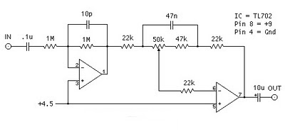
The following is megabass circuit schematic (rangkaian megabass) . The megabass circuit is a modified Baxandall tone control with no bass cut and no treble control. It boosts frequencies from about 30Hz to 160Hz can boost by 14dB.

Bass Booster Schematics
Bass Booster with TL072

Note:
The input capacitor can be replaced with a .01uf cap if you wish.
The 10pf capacitor is optional and will start rolling off everything over 15kHz. 5pf will double this to 31kHz.
The tone control requires a low impedence input. If you already have a low impedence input, the input buffer can be removed. However, the output is inverted.
The opamp is not critical. A 4558 would be just fine.
I do not show the parts for the +4.5 reference. Here is the +4.5 voltage divider I used.
IC A4558 Pinning

The A4558 is a monolithic Integrated Circuit designed for dual operational amplifier.

Absolute maximum ratings of A4558 Ap-amp
Supply voltage VCC 20 or ±10 V
Differential input voltage VIND 20 V
Input voltage VIN ±10 V
Power Dissipation PD 300 mW
Operating temperature Topr -45 ~ +85 °C
Storage temperature Tstg -55 ~ +150 °C
ReadMore..

Tuesday, April 9, 2013

Logic Probe With Sound

This logic probe can be selected to operate on TTL or CMOS logic levels, depending on switch S1. A string of resistors associated with switch S1 sets the threshold levels for a window comparator comprising IC1a and IC1b. Depending on whether the level applied to the probe is high or low, the window comparator turns on LED1 (high) or LED2 (low). The 1.2M and 680k resistors set the probe signal to a midrange value when the probe is open-circuit, thereby preventing either LED from being lit.

Logic probe with sound circuit schematic

If a pulse signal is present, the output of IC1a will toggle the clock input of flipflop IC2a. This drives LED3 which either lights for each pulse or continuously, depending on the setting of switch S2. Finally, the outputs of IC1a & IC1b are connected by diodes D5 & D6 to the base of transistor Q1 which is connected to the Reset input of flipflop IC2b. This has a piezo sounder (not buzzer) connected between its Q and Q-bar outputs so that it produces a sound which echoes the input pulse signal.
ReadMore..

Monday, April 8, 2013

1W Stereo Amplifier With Voltage Regulators

A simple
stereo audio amplifier is built around two 7905 negative-voltage
regulators (IC1 and IC2) and a few discrete components. The circuit
will also work with other 79XX regulators if appropriate power supply
is used. Regulator IC 7905 works as an amplifier for the voltages
applied to common pin2 (Ground or GND). Also check the LM317 audio
amplifier, another interesting circuit.The minimal voltage drop over the
standard 7905 is around 2V and it depends on the output current.
Feedback resistors in the IC set the gain of the channel internally.
The amplifier is a class-A audio amplifier. The minimal applicable
value of R3 for the regulator 7905 is 8.2 to 10 ohms per 5W.

7905 1 Watt Audio Amplifier Schematic

1watt 7905 stereo amplifier circuit schematic
If
the required output current for LS1 is below 100 mA, the value of
resistor R3 can be 33 to 51 ohms per watt. The circuit works with any
load resistance (R3 in parallel with LS1 as the load) under the
condition that the regulator is not overloaded with current and power
dissipation. However, it is preferable to use a loudspeaker with a high
resistance (8 ohms, 16 ohms or more). The amplifier works well with
low-impedance headphones having a resistance of 24 to 32 ohms. The
voltage difference between the ground pin of 7905 and the output pin is
fixed internally.
S2 is the on/off switch. Switch S1 is for
mono/stereo selection. When switch S1 is closed, the amplifier works as
a two-way mono amplifier. If S1 is open, the amplifier works as a
stereo amplifier. If no input signal is applied, the DC voltage on the
output of the regulator 7905 should be around –5V, which depends to
some extent on the value of VR1. The maximum output current of 7905 can
be up to 1A and the maximum power dissipation is up to 15W. Mount the
regulator IC 7905 on a heat-sink with
ReadMore..

Friday, April 5, 2013

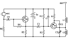
Simple FM transmitter with 2N3904

simple FM transmitter
In this section discuss about the series of mini fm transmitter, with broadcast coverage of about 300-400 meters. when using a 9 volt working voltage, the transmit power of about 300 meters and when using the working voltage 12 volts, the range of about 400-450 meters, depending on the antenna you use.

This scheme of simple fm transmitter
simple FM transmitter

For L1 and L2 windings 5 times the wrap, you can use a pen to fill melilitnya so neat and after lepaslah content of these pens. C5 is used for placement of broadcasting frequencies, can be tuned between 88-108 mhz, to reach further use steering antenna or Yagi antenna.

Part List
C1 = 0.001uF
C2 = 5.6pF
C3 = 10uF
C4 = 10uF
C5 = 3 - 18pF Adjustable capacitor
R1 = 270R
R2 = 4.7K
R3 = 10K
R4 = 100K
R5 = 4.7K
R6 = 4.7K
Q1 = 2N2222A
Q2 = 2N3904
L1 = 5 turn
L2 = 5 turn
ReadMore..

Thursday, April 4, 2013

Logic PSU With Over Voltage Protection

A simple 5 Volt regulated PSU featuring overvoltage protection. The 5 volt regulated power supply for TTL and 74LS series integrated circuits, has to be very precise and tolerant of voltage transients. These ICs are easily damaged by short voltage spikes. A fuse will blow when its current rating is exceeded, but requires several hundred milliseconds to respond. This circuit will react in a few microseconds, triggered when the output voltage exceeds the limit of the zener diode. This circuit uses the crowbar method, where a thyristor is employed and short circuits the supply, causing the fuse to blow. This will take place in a few microseconds or less, and so offers much greater protection than an ordinary fuse.

Circuit diagram:
Logic PSU With Over-Voltage Protection Circuit Diagram

If the output voltage exceed 5.6Volt, then the zener diode will conduct, switching on the thyristor (all in a few microseconds), the output voltage is therefore reduced to 0 volts and sensitive logic ICs will be saved. The fuse will still take a few hundred milliseconds to blow but this is not important now because the supply to the circuit is already at zero volts and no damage can be done. The dc input to the regulator needs to be a few volts higher than the regulator voltage. In the case of a 5v regulator, I would recommend a transformer with secondary voltage of 8-10volts ac. By choosing a different regulator and zener diode, you can build an over voltag trip at any value.
ReadMore..