Friday, December 27, 2013

IR Remote Control Tester

Here’s a simple, low cost, and easy to construct infrared remote control tester. The tester is built around an easily available infrared receiver module (TSOP 1238).

 IR Remote Control Tester Circuit diagram:

Schematic diagram of IR remote control tester
Normally, data output pin 3 of the IR receiver module is at a high level (5 volts)and as such driver transistor T1 is in cut-off state. Whenever the IR receiver module receives a valid (modulated) infrared signal, its data output pin goes low in synchronism with the received infrared bursts. As a result, transistor T1 conducts during negative pulse period and the.LED blinks to indicate reception of signals from the remote such as TV remote control. A miniature active buzzer is connected at the collector of transistor T1 for audio indication.


Proposed enclosure with front-panel

The 5V DC for energizing the circuit is directly derived from the 230V AC mains supply. Unlike the conventional resistive voltage divider, a capacitive potential divider is used here, which does not radiate any heat and makes the tester quite compact. Another advantage of this tester is no false triggering due to the ambient light or electronic ballast-operated tubelights. A suggested enclosure for the circuit is shown in Fig. 2.
Source :  http://www.ecircuitslab.com/2011/06/schematic-diagram-of-ir-remote-control.html
ReadMore..

Thursday, December 26, 2013

Touch Sensitive Light Dimmer

With IC SLB0586A from Siemens you can build a simple touch light dimmer circuit that will allow you to adjust the lamp intensity. Together with a TIC206D triac, it enables smooth regulation of light intensity from a bulb of 10W – 400W. A coil of 100µH/5A is required to suppress switching noise.

The voltage supply is obtained through R2, C2, D1 and C3 and is about 5.3V below the network potential. The touch sensor that is used to drive the IC is connected at pin 5 through two 4.7MΩ resistors, R5 and R6, in order to ensure user security.

In the adjustable touch lamp schematic we can see three selection connection , for selecting one of three modes of the IC. When the B connection is used, the light will always be ON at the last level that we used. With A or C connection the light will be ON at the minimum intensity. With B or C, the purpose of regulation is reversed with each use.

Schematic of the adjustable light with touch sensor
Circuit Project: Touch light dimmer circuit
Touch Sensitive Light Dimmer Circuit Diagram


When the sensor is touched for a short period of time (50 – 400 ms), the lamp will be ON or OFF. If the sensor is touched for a longer period of time it will start the regulation process. Warning! This touch light dimmer circuit has some points where lethal 220V is present, please do not try this project if you are not qualified.
ReadMore..

Wednesday, December 25, 2013

Simple Infra red Receiver

This very simple infra-red receiver is intended to form an infra-red remote control system with the simple infra-red transmitter described in this site. The system does not use any kind of coding or decoding, but the carrier of the transmitter is modified in a simple manner to provide a constant switching signal. Since the receive module, IC1, switches from low to high (in the quiescent state, the output is high) when the carrier is received for more than 200 milliseconds, the carrier is transmitted in the form of short pulse trains. This results in a pulse at the output of the receiver that has a duty cycle which is just larger than 12.5%. The carrier frequency used in the system is 36 kHz, so that the output frequency of IC1 is 281.25 Hz.

Infra-red Receiver Circuit diagram :


This signal is rectified with a time constant that is long enough to ensure good smoothing, so that darlington T1 is open for as long as the received signal lasts. A drawback of this simple system is that it may pick up signals transmitted by another infra-red (RC5) controller. In this case, only the envelopes of the pulse trains would appear at the output of T1. This effect may, of course, be used intentionally. For instance, the receiver may be used to drive an SLB0587 dimmer. Practice has shown that the setting of the SLB0587 is not affected by the RC5 pulses. The receiver draws a current of about 0.5 mA.

Source : www.ecircuitslab.com/2011/05/infra-red-receiver-circuit.html
ReadMore..

Tuesday, December 24, 2013

Super Universal Battery Charger Circuit Diagram

The Super Universal Battery Charger Circuit Diagram output voltage is adjustable and regulated, and has an adjustable constant-current charging circuit that makes it easy to use with most NiCad batteries. The charger can charge a single cell or a number of series-conoected cells up to a maximum of 18 V. 

Power transistors Ql and Q2 are conoected as series regulators to control the battery charger`s output voltage and charge-current rate. An LM317 adjustable voltage regulator supplies the drive signal to the bases of power transistors Ql and Q2. Potentiometer R9 sets the output-voltage level. A current-sampling resistor, R8 (a 0.1-!J, 5-W unit), is conoected between the negative output lead and circuit ground. For each amp of charging that flows through R8, a 100 mV output is developed across it. 

The voltage developed across RS is fed to one input of comparator U3. The other input of the comparator is connected to variable resistor RIO. As the charging voltage across the battery begins to drop, the current through RS decreases. Then the voltage feeding pin 5 of U3 decreases, and the comparator output follows, turning Q3 back off, which completes the signal`s circular path to regulate the battery`s charging current. The charging current can be set by adjusting RlO for the desired current. The circuit`s output voltage is set by R9. 

Super Universal Battery Charger Circuit Diagram

Super Universal Battery Charger Circuit Diagram


ReadMore..

Monday, December 23, 2013

12V Touch Switch Exciter

This circuit is designed to generate a 20KHz pseudo sine wave signal that can power about 50 remote touch activated switch circuits.  It can support a cable length of about 2500 feet.  A typical remote switch circuit is also shown as well as a receiver circuit for those switches.

Source: DiscoverCircuits
ReadMore..

Sunday, December 22, 2013

Simple Video Amplifier

The video amplifier in the diagram is a well-known design. Simple, yet very useful, were it not for the ease with which the transistors can be damaged if the potentiometers (black level and signal amplitude) are in their extreme position. Fortunately, this can be obviated by the addition of two resistors.

Circuit diagram :

Simple Video Amplifier-Circuit Diagram Simple Video Amplifier Circuit Diagram


If in the diagram R 3 and R 4 were direct connections, as in the original design, and P 1 were fully clockwise and P 2 fully anticlockwise, such a large base current would flow through T 1 that this transistor would give up the ghost. Moreover, with the wiper of P 2 at earth level, the base current of T 2 would be dangerously high. Resistors R 3 and R 4 are sufficient protection against such mishaps, since they limit the base currents to a level of not more than 5 mA.

Shunt capacitor C 4 prevents R 4 having an adverse effect on the amplification.

ReadMore..

Saturday, December 21, 2013

Build a Inexpensive Isolation Transformer Circuit Diagram

Build a Inexpensive Isolation Transformer Impromptus Setup Circuit Diagram. Using two 12-V filament or power transformers, an impromptu isolation transformer can be made for low-power (under 50 W) use in testing or servicing. SOI is an ordinary, duplex ac recept-able. Use heavy-wire connections between the 12-V windings because several amperes can flow.

Inexpensive Isolation Transformer Circuit Diagram


Inexpensive Isolation Transformer Circuit Diagram

ReadMore..

Friday, December 20, 2013

AC 220V Mains Powered Emergency Light and Alarm

This circuit is permanently plugged into a mains socket and NI-CD batteries are trickle-charged. When a power outage occurs, the lamp automatically illuminates. Instead of illuminating a lamp, an alarm sounder can be chosen. When power supply is restored, the lamp or the alarm is switched-off. A switch provides a "latch-up" function, in order to extend lamp or alarm operation even when power is restored.

Emergency Light and Alarm Circuit Diagram

Parts List:


R1 = 220K
R2 = 470R
R3 = 390R
R4 = 1.5K
R5 = 1R
R6 = 10K
R7 = 330K
R8 = 470R
R9 = 100R
D1 = 1N4007
D2 = 1N4007
D3 = 1N4007
D4 = 1N4007
D5 = 1N4007
D6 = Led
D7 = 1N4148
Q1 = BC547
Q2 = BC327
Q3 = BC547
Q4 = BC547
Q5 = BC327
C1 = 330nF-400V
C2 = 10uF-63V
C3 = 100nF-63V
C4 = 10nF-63V
LP1 = 2.5V-300mA Torch Lamp Bulb
PL1 = Male Mains Plug
SW1 = SPST Switches
SW2 = SPST Switches
SW3 = SPDT Switches
SPKR = 8 Ohms Loudspeaker
B1 = 2.5V Battery (two AA NI-CD rechargeable cells wired in series)

Mains voltage is reduced to about 12V DC at C2s terminals, by means of the reactance of C1 and the diode bridge (D1-D4). This avoids the use of a mains transformer. Trickle-charging current for the battery B1 is provided by the series resistor R3, D5 and the green LED D6 that also monitors the presence of mains supply and correct battery charging.

Q2 & Q3 form a self-latching pair that start operating when a power outage occurs. In this case, Q1 biasing becomes positive, so this transistor turns on the self latching pair. If SW3 is set as shown in the circuit diagram, the lamp illuminates via SW2, which is normally closed; if set the other way, a square wave audio frequency generator formed by Q4, Q5 and related components is activated, driving the loudspeaker.

If SW1 is left open, when mains supply is restored the lamp or the alarm continue to operate. They can be disabled by opening the main on-off switch SW2. If SW1 is closed, restoration of the mains supply terminates lamp or alarm operation, by applying a positive bias to the Base of Q2.

Note:


Close SW2 after the circuit is plugged.

Warning!


The circuit is connected to 230Vac mains, then some parts in the circuit board are subjected to lethal potential!. Avoid touching the circuit when plugged and enclose it in a plastic box.

ReadMore..

Thursday, December 19, 2013

Solar Power Supply

This circuit delivers either 4.8 or 7.2 V regulated at 15 mA with a 3-V input from a bank of photocells. Rl should be 453 kQ for a 7.2-V output and 274 РЁ for a 4.8-Vdc output. Regulator efficiency is around 70%. This should be considered when selecting suitable solar cells.

Solar Power Supply Circuit diagram :


ReadMore..

Wednesday, December 18, 2013

The ordering quantity of this order of Cell Phone Jammers is large enough

The document of  Cell Phone Jammers  will contain the important product information of  Cell Phone Jammers  .
The laser has been widely applied to the laser welding, laser cutting, laser drilling (including the slant-hole, different holes, plaster hole, perforated tipping paper, perforated steel, perforated packaging and printing, etc.), laser hardening, laser heat treatment, laser marking, glass engraving, laser trimming, laser lithography, laser system, film, laser film processing, laser packages, laser repair circuits, laser routing technology, laser cleaning.
Periodic illegible: often drum charge roller coating or contamination, watermarks, mimeo, fingerprints often cause this defect. Grapes: It is the same as the overlapping coins appear in the printed materials of a defect, no rules, and difficult to repeat, is caused by bad drum ground. Background scattering: refers to the text or unwanted lines around the black specks, toner from the magnetic roller coating or bad cause. Drum overheating (referring to a sense of high) may also cause this defect. Wave background (tiger grouper): wavy black version in white or white on black version or in the form of half-tone version. Several more kinds of payment method of  Cell Phone Jammers  will be added for this online store of  Cell Phone Jammers  .
Usually magnetic roller sleeve coating defects or due to prolonged low-density printing, magnetic bond caused by the magnetic roller sleeve. Hollow words: refers to the text or images is missing strokes on the reasons: toner itself is the problem. Dark pink with bad. Magnetic roller coating problems. Print media over the surface of the light, perfect. Paper with the negative. Irregular vertical black spots: the deformation caused by the sealing of the waste toner smears scattered. As the accumulation of too much toner on the magnetic roller, causing leakage of powder. Coloration: with a variety of factors: the toner itself is the problem. Toner, magnetic roller with the problem. Flour knife aging. Magnetic roller wear. Drums to life. High humidity or moisture absorption media. The detailed information of  Cell Phone Jammers  contains the ordering quantity of  Cell Phone Jammers  .
Bottom ash: bottom ash refers to prints blank zone in the mist toner, but also with a variety of factors: aging scraper. Charge roller fouling. Toner problem. Drum fatigue, to life. Low temperature and dry environment. Print media bad. Charge roller wear. Fixing is not strong: refers to the printed text or images on the product that is out of touch. The reasons are: toner softening point higher than the machines fusing temperature. Print media too thick or too light surface. Before cleaning the printer, be sure to carefully read the printer user manual to follow any special procedures and warnings. The ordering quantity of this order of  Cell Phone Jammers  is large enough.
ReadMore..

Tuesday, December 17, 2013

DC Fan Controller

This circuit is ideal to control the cooling fan of heat generated electronic gadgets like power amplifiers. The circuit switches on a fan if it senses a temperature above the set level. The fan automatically turns off when the temperature returns to normal. The circuit uses an NTC (Negative Temperature Coefficient) Thermister to sense heat. NTC Thermister reduces its resistance when the temperature in its vicinity increases.

IC1 is used as a voltage comparator with two potential dividers in its inputs. Resistor R1 and VR1 forms one potential divider connected to the non inverting input of IC1 and another potential divider comprising R2 and the 4.7K Thermistor supplying a variable voltage to the inverting input of IC1. VR1 is adjusted so as to give slightly lesser voltage at the non inverting input than the inverting input at room temperature.

DC Fan Controller Circuit


In this state, output of IC1 will be low and the Fan remains off. When the temperature near the Thermister increases, its resistance decreases and conducts. This drops the voltage at pin 2 of IC1 and its output becomes high. T1 then triggers and fan turn on. Red LED indicates that fan is running. Capacitor C1 gives a short lag before T1 turns on to avoid false triggering and to give proper bias to T1.

DC fan can be the one used in Computer SMPS. Keep the Thermistor near the heat sink of the Amplifier PCB and switch on the amplifier for 10 minutes. Then adjust VR1 till the Fan stop running.When the temperature rises, Fan will automatically switch on.
ReadMore..

Thursday, October 10, 2013

Short Circuit Protection With A MOSFET

If you have an application in which a MOSFET is already used to switch a load, it is relatively easy to add short-circuit or overload protection. Here we make use of the internal resistance RDS(ON), which produces a voltage drop that depends on the amount of current flowing through the MOSFET. The voltage across the internal resistance can be sensed using simple comparator or even a transistor, which switches on at a voltage of around 0.5V. You can thus avoid the use of a sense resistor (shunt), which usually produces an undesirable extra voltage drop. The comparator can be monitored by a microcontroller. In case of an overload, the software can initiate suitable countermeasures (PWM regulation, alarm, emergency stop etc.). It is also conceivable to connect the comparator output directly to the gate of the MOSFET, in order to immediately cut off the transistor in case of a short circuit.

Short-Circuit Protection With A MOSFET Circuit Diagram
ReadMore..

Wednesday, October 9, 2013

Yes No Indicator Has Zero Standby Current

This circuit produces a random "Yes" or "No" with a single button press - indicated by the illumination of a red or green LED. The circuit has two advantages over similar circuits. First, it uses just a single momentary contact pushbutton, so no on-off switch is required. When the pushbutton is pressed, an oscillator comprising the 10nF capacitor and 22kΩ resistor at pins 1 & 2 is almost immediately stopped by FET Q1, which pulls the oscillators timing capacitor to the positive rail. However, the 220nF capacitor and 470kΩ resistor in the gate circuit of Q1 introduce a tenth of a seconds delay, so that about 250 oscillations take place before the clock is stopped.

Due to variations in charge on the circuits capacitors, as well as voltage and temperature variations, and the unpredictability of when the pushbutton will be pressed, randomness is assured. The circuit has a high degree of randomness because it takes advantage of a near-perfect complementary square waveform at pins 10 and 11 of the 4047 IC. The oscillator frequency (available at pin 13) is passed through an internal divide-by-2 circuit in the 4047. This appears at pin 10 (Q), and is inverted at pin 11 (Q-bar), thus assuring a near perfect 50:50 duty cycle for the two LEDs.
Yes-No indicator has zero standby current circuit schematic
Note:

However, that the "impartiality" of the circuit is partly contingent on the value of the 10nF capacitor and on a reasonably equal current flow through both LEDs. Over five trials, the Yes-No Indicator scored 142 Yes, 158 No, with Yes falling behind No in the fourth trial. Because the circuit only works while switch S1 is pressed, standby current is zero, therefore a miniature 12V battery may be used to power it. In this case the circuit could be used thousands of times before the battery would run flat. The circuit has a further potential use. If the LEDs are omitted and a piezo (capacitive) sounder is wired directly to pins 10 and 11, it will produce a loud beep when equipment is turned on, and will continue to draw less than 0.5mA until it is switched off. The frequency of the beep may be changed by altering the value of the 10nF capacitor and its duration by altering the value of the 220nF capacitor.
ReadMore..

Tuesday, October 8, 2013

Headphone Amplifier Using Discrete Components

An amplifier to drive low to medium impedance headphones built using discrete components.

Both halves of the circuit are identical. Both inputs have a dc path to ground via the input 47k control which should be a dual log type potentiometer. The balance control is a single 47k linear potentiometer, which at center adjustment prevents even attenuation to both left and right input signals. If the balance control is moved towards the left side, the left input track has less resistance than the right track and the left channel is reduced more than the right side and vice versa. The preceding 10k resitors ensure that neither input can be "shorted" to earth.

Headphone Amplifier Circuit DiagramAmplification of the audio signal is provided by a single stage common emitter amplifier and then via a direct coupled emitter follower. Overall gain is less than 10 but the final emitter follower stage will directly drive 8 ohm headphones. Higher impedance headphones will work equally well. Note the final 2k2 resistor at each output. This removes the dc potential from the 2200u coupling capacitors and prevents any "thump" being heard when headphones are plugged in. The circuit is self biasing and designed to work with any power supply from 6 to 20 Volts DC.
ReadMore..

Monday, October 7, 2013

14W CLASS A AMPLIFIER USING 2N3055 ELECTRONIC DIAGRAM

14W CLASS A AMPLIFIER USING 2N3055 ELECTRONIC DIAGRAM

Why Class A ? Because , when biased to class A, the transistors are always turned on, always ready to respond instantaneously to an input signal. Class B and Class AB output stages require a microsecond or more to turn on. The Class A operation permits cleaner operation under the high-current slewing conditions that occur when transient audio signal are fed difficult loads. His amplifier is basically simple, as can be seen from the block diagram.
ReadMore..

Sunday, October 6, 2013

You Have Mail!

If your letterbox is some distance from your house, you will find a monitoring device useful to indicate when new post has arrived. This can take the form of a US-style visible flag; a more modern alternative uses a 433 MHz radio transceiver. The big advantage of the solution presented here is that is can use an existing two-core bell cable, without requiring any further power source. The arrival of post is signalled by a blinking LED; for added effect, a digital voice recorder can also be connected which will, at regular intervals, announce the fact that the letterbox needs emptying. The device is silenced by a reset button.

The circuit uses one half-cycle of the AC supply to power the bell or buzzer, and the other half-cycle for the post indicator. Suitably-oriented diodes in the device and in the letterbox ensure that the two signals are independent of one another (Figure 1). The bell current flows from K1.A through D3, bell-push S2, D1 and the relay back to K1.B. C1 provides adequate smoothing of the current pulses to ensure that the relay armature does not vibrate. The bell is operated by the normally-open relay contact. If the bell is actually a low-current piezo buzzer, then it can be connected directly and the relay dispensed with.

During the half-cycle for the letterbox monitor current flows from connection K1.B on the bell transformer through current-limiting resistor R1, the LED in the optocoupler, reed contact S1 (a micro-switch can also be used) and D2 and finally back to K1. If the reed contacts are closed, the LED in the optocoupler will light and switch on the phototransistor. A positive voltage will then appear across R3 which will turn the thyristor on via C6. The red LED will indicate that post has arrived. Pressing S3 shorts out the thyristor, reducing the current through it below the holding value. A small extra circuit can be added to provide continuous letterbox monitoring.

You Have Mail!This takes the form of a voice recorder whose ‘play’ button is operated by transistor T1. T1 in turn is driven by a 555 timer IC. In the usual 555 timer circuit, where the device is configured as an astable multi-vibrator, the mark-space ratio cannot be set with complete freedom. Here two diodes provide separate charge and discharge paths for capacitor C4. When capacitor C4 is charging, D5 conducts and D4 blocks: the charge rate is determined by R5. When discharging, D4 conducts and R6 and the potentiometer determine the rate. The values shown give a pulse length of approximately 0.5 s with a delay of between 15 s and 32 s.

The short pulse is sufficient to trigger the voice recorder module via transistor T1 connected across its ‘play’ button. The voice recorder module (e.g. Conrad order code 115266) is designed to run from a 6 V supply. The maximum recording time is 20 s and the current consumption is 20 mA when recording and between 40 mA and 60 mA when playing back. Since our supply is at 8 V, the excess voltage must be dropped using between 1 and 3 series-connected 1N4148 diodes (shown as Dx in the circuit diagram). The final voltage should be checked using a multimeter. Alternatively, a 7806 can be used without suffering a significant loss in volume.

If it is desired to use a piezo buzzer to provide an acoustic signal, the pulse length should be increased to at least 2s. In this case, R5 should be increased to 560 kΩ or 680 kΩ: the pulse length, t on, is 0.7.R5.C4, and the interval between pulses, t off, is 0.7. (R6+R7).C4. Suitable buzzers are available with a wide range of rated voltages.
ReadMore..

Saturday, October 5, 2013

12V Speed Controller Dimmer

This handy circuit can be used as a speed controller for a 12V motor rated up to 5A (continuous) or as a dimmer for a 12V halogen or standard incandescent lamp rated up to 50W. It varies the power to the load (motor or lamp) using pulse width modulation (PWM) at a pulse frequency of around 220Hz.

SILICON CHIP has produced a number of DC speed controllers over the years, the most recent being our high-power 24V 40A design featured in the March & April 2008 issues. Another very popular design is our 12V/24V 20A design featured in the June 1997 issue and we have also featured a number of reversible 12V designs.

Circuit looks like:

12V-speed-controller-lamp-dimmer-circuit

For many applications though, most of these designs are over-kill and a much simpler circuit will suffice. Which is why we are presenting this basic design which uses a 7555 timer IC, a Mosfet and not much else. Being a simple design, it does not monitor motor back-EMF to provide improved speed regulation and nor does it have any fancy overload protection apart from a fuse. However, it is a very efficient circuit and the kit cost is quite low.

Parts layout:

parts-layout-12V-speed-controller-lamp-dimmer-circuit

Connection diagram:

12V-motor-speed-controller-lamp-dimmer-circuit

There are many applications for this circuit which will all be based on 12V motors, fans or lamps. You can use it in cars, boats, and recreational vehicles, in model boats and model railways and so on. Want to control a 12V fan in a car, caravan or computer? This circuit will do it for you.

Circuit diagram:

12V-speed-controller-lamp-dimmer-circuit-diagram

The circuit uses a 7555 timer (IC1) to generate variable width pulses at about 210Hz. This drives Mosfet Q3 (via transistors Q1 & Q2) to control the speed of a motor or to dim an incandescent lamp.
Halogen lamps:
While the circuit can dim 12V halogen lamps, we should point out that dimming halogen lamps is very wasteful. In situations where you need dimmable 12V lamps, you will be much better off substituting 12V LED lamps which are now readily available in standard bayonet, miniature Edison screw (MES) and MR16 halogen bases. Not only are these LED replacement lamps much more efficient than halogen lamps, they do not get anywhere near as hot and will also last a great deal longer.

Source: Silicon Chip 15 November 2008

ReadMore..

Friday, October 4, 2013

Video Tracer Circuit Diagram

This circuit was designed as an aid to installers and maintainers of video systems. It is basically a video sync separator (IC1) followed by a LED and buzzer driver (IC2, Q1 & Q2). In use, the device is connected to a video cable and if there is video present, the LED will flash at about 10Hz. If there is no video, the LED flashes briefly every couple of seconds. A buzzer can also be switched in to provide an audible indication. The buzzer is particularly useful when tracing cabling faults or trying to find a correct cable amongst many, where it is difficult to keep an eye on the LED.
Another use for the buzzer option is to provide a video fault indication. For example, it could be inserted in bridging mode, with switch S1 in high impedance mode (position 2) across a video line and set to alarm when there is no video present. If someone pulls out a cable or the video source is powered off, the alarm would sound. IC1 is a standard LM1881 video sync separator circuit and 75Ω termination can be switched in or out with switch S1a. The other pole of the switch, S1b, turns on the power. The composite sync output at pin 1 is low with no video input and it pulses high when composite sync is detected.
Circuit diagram:
video-tracer-circuit-for-trouble-shooting1
These pulses charge a 100nF capacitor via diode D1. When there is no video at the input, oscillator IC2b is enabled and provides a short pulse every couple of seconds to flash the LED. The duty cycle is altered by including D2, so that the discharge time for the 10μF capacitor is much shorter than the charge time. The short LED pulse is used as a power-on indicator drawing minimal average current. When video is present at the input, IC2b is disabled and IC2d is enabled. The output of IC2d provides a 10Hz square wave signal to flash the LED. The buzzer is controlled by switch S2. In position 2 the buzzer will sound when there is video at the input and in position 1 the buzzer will sound when there is no video at the input.
Author: Leon Williams - Copyright: Silicon Chip Electronics
ReadMore..

Thursday, October 3, 2013

1993 VW Passat Electrical Circuit Diagram

1993 VW Passat Electrical Circuit Diagram
The Part of 1993 VW Passat Electrical Circuit Diagram: automatic control unit,  fuse/relay panel and
emergency lights, fuse/relay panel and fresh air blower switch, Engine control module and ignition coil, console switch, power windows, ABS control unit and ABS hydraulic unit, fuse relay panel and instrument cluster, and taillight, fuse/relay panel and headlight switch, automatic sol, fuse/relay panel and ignition switch, Engine control module.
ReadMore..

Wednesday, October 2, 2013

Voltage Regulator Calculation

Before you can design an adjustable voltage regulator into your circuit, or do a redesign, you need to calculate the values for two resistors. This is not difficult in itself, but actually finding the right resistors may pose problems. Fortunately a trick is available to make it all much easier. With most adjustable voltage regulators like the LM317 and LM337, the input voltage has to be 1.2 to 1.25 volts above the desired output voltage. This is because the voltage at the ADJ (adjust) input is internally compared to a reference voltage with that value. The reference voltage always exists across R1.
Voltage Regulator CalculationTogether with preset R2 it determines the current flowing through the ADJ pin, as follows: Vout = VREF [1+(R2/R1)]+I ADJ R2 If for the sake of convenience we ignore I ADJ, enter the reference voltage (1.2 V) and for R1 select a value of one thousand times that voltage (i.e., 1.2 k?) then the equation is simplified to: R2 = 1000 (Vout – 1.2) In practice, simply determine the voltage drop across R2 (output voltage minus reference voltage) and you get your resistance value directly in kilo-ohms. For example, for 5 V R2 becomes 5–1.2 = 3.8 k? which is easiest made by connecting 3.3k and 470R resistors in series. In the case of relatively low voltages, smaller resistor values are recommended. This is because sufficient current needs to flow to enable the voltage regulator to do its job. A simple solution is to choose, say, 120 ? for R1. R2 then becomes: R2 = 100 (Vout – 1.2)
ReadMore..

Tuesday, October 1, 2013

Fuse Box BMW 318i 1991 Diagram

Fuse Box BMW 318i 1991 Diagram - Here are new post for Fuse Box BMW 318i 1991 Diagram.

Fuse Box BMW 318i 1991 Diagram


Fuse Box BMW 318i 1991 Diagram

Fuse Panel Layout Diagram Parts: seat heating, high beam headlight, auxiliary fan, sliding roof, flashing turn indicator, mirror control, wiper, washer, horn, brake light, cruise control, heated rear window, GLOVEBOX, LUGGAGE COMPARTMENT LIGHT, ON BOARD COMPUTER.instruments, on board computer, reversing light, fuel supply pump, radio, check control and instrument, fog light, fog light, cigar lighter, central locking, door lock heating, hazard warning flasher, parking light, license plate light.
ReadMore..

Monday, September 30, 2013

9V DC Adapter With Battery Backup

With just a low cost DC adapter and the circuit described here it is possible to build a low cost stabilized, uninterruptable 9V supply. On the grounds of safety and economy, a simple unstabilized 12V D.C. adapter is used as the power source, a universal adapter with its output set to 12 V will do equally well. The output voltage of an adapter under low load conditions (up to approximately 1/3 of the rated output current) is over 15 V, even at the rated output current, there will be sufficient voltage to supply a 9 V voltage regulator. The rating of the DC adapter should be chosen according to the output current required at 9V. Common values are 300mA, 500mA and 1A.

The 9V voltage regulator used in this circuit has a built in thermal shutdown mechanism so that if too much current is drawn from the device, it simply turns off as it overheats and will not supply any current until the case temperature returns to normal. If the unit is intended to supply more than say 150-200mA then to prevent thermal shutdown it will be necessary to fit a heatsink to the voltage regulator. The rule of thumb used to calculate the size of heatsink is that you should be able to touch it during operation at maximum load, without burning you finger. When choosing the DC adapter, it is always better to select one with a higher current rating than is needed this will ensure that its output voltage is high enough to be able to also charge the 12V cells.

DC Adapter with Battery Backup Circuit DiagramAs long as mains voltage is on the DC adapter, the voltage across C1 will be higher than the voltage of the cells. Charging current will flow through R1 and D1 to the cells. Current also flows to the voltage regulator and out to the load connected at the output. Diode D2 in this situation will not conduct because the voltage at its cathode is greater than that at its anode When the mains voltage fails or is turned off, diode D2 conducts and current will now flow from the Nickel Cadmium cells to the voltage regulator, thereby automatically keeping the output voltage at 9V. The value of resistor R1 is chosen so that a charging current to the cells is not greater than 1/10th of the cells capacity (if the cells are rated at 1100mAh, the charging current must not exceed 110mA).

From the point of view of cell longevity it is better to reduce this charging current even further (1/20 or 1/50 C). When calculating this resistor, the value of the no-load voltage should be used. This will give the highest charging current. To calculate the charging current using R1 with a value of 180 Ω. The cells measure 13.8 V when fully charged and the no-load output voltage of the DC adapter is 17V. Charging current is given by the formula: (17V – 13.8V – 0.7V) / 180 = 13.9mA. Substituting the actual measured values in this formula will enable you to calculate the value of R1 to give the correct charging current for the cells.
ReadMore..

Sunday, September 29, 2013

Simple Knock Alarm With Piezo Sensor

This circuit uses a thin piezoelectric sensor to sense the vibrations generated by knocking on a surface; eg, a door or table. Basically, it amplifies and processes the signal from the sensor and sounds an alarm for a preset period. In operation, the piezoelectric sensor converts mechanical vibration into an electrical signal. This sensor can be attached to a door, a cash box, cupboard, etc using adhesive. A 1-1.5m long shielded cable can then be connected between the sensor plate and the input of the circuit. The signal generated by the sensor is amplified by transistors Q1-Q3 which are wired as common-emitter amplifiers.

Simple knock alarm with piezo sensor circuit schematic

The signal is then rectified by diode D1 and amplified by transistors Q4-Q6. As shown, the output from Q6s collector is fed to pin 4 (reset) of 555 timer IC1. This is wired as an astable multivibrator. Each time Q6 turns on, its collector goes high and IC1 activates and produces an alarm tone in the speaker. The alarm automatically turns off 10s after knocking ceases - ie, the time taken for the 22µF capacitor on Q4s emitter to discharge. Finally, note that it may be necessary to adjust the 470O resistor in Q6s collector circuit to ensure that IC1 remains off in the absence of any perceptible knock. A value somewhere between 220O and 680O should be suitable.
ReadMore..

Saturday, September 28, 2013

Headlight Reminder

With the storm season recently upon us, it’s not uncommon to switch car headlights on during the daytime. Unfortunately, it’s easy to forget to turn them off again when parking, with the result being a flat battery. This circuit will sound an alarm if the ignition switch is moved to the "off" position while the car lights are on, reminding you to turn the lights off before leaving the vehicle.
The circuit is simple but effective. A 555 timer (IC1) is configured as a free-running oscillator to drive a small piezo transducer. The pitch of the transducer is set by the resistor and capacitor connected to pins 2 & 6. Power for the 555 is derived from the dashboard lighting circuit. However, the piezo does not sound during normal operation, because the 555’s reset input (pin 4) is held low by transistor Q1.
Circuit diagram:
headlight-reminder-circuit-diagram
This transistor is switched on whenever accessory power is present, pulling its collector towards ground (0V). If the ignition is switched off but the lighting circuit remains powered, the loss of accessory power results in Q1 switching off and releasing the reset signal to IC1, sounding the alarm. A 220Ω resistor in series with the piezo protects the 555’s output (pin 3). Although most piezo elements have relatively high impedance, this drops as the frequency increases due to their capacitive nature.
The square-wave output on pin 3 includes many harmonics, some extending well into the ultrasonic range. The unit fits easily into a small plastic box. I spliced mine into the wiring running to the cigarette lighter, which includes both accessories and panel lamp circuits as well as a chassis ground wire. The result fits neatly behind the ashtray, with no chassis bashing required!
Author: Bruce Colledge - Copyright: Silicon Chip Electronics
ReadMore..

Friday, September 27, 2013

Isolated Fuse Fail Indicator

This circuit uses standard components and shows a method of indicating the fuse status of mains powered equipment while providing electrical isolation from the mains supply. A standard miniature low power mains transformer (e.g. with an output of around 6 V at 1.5 VA) is used as a ‘sense’ transformer with its primary winding (230 V) connected across the equipment’s input fuse so that when the fuse blows, mains voltage is applied to the transformer and a 6 V ac output voltage appears at the secondary winding. The 1N4148 diode rectifies this voltage and the LED lights to indicate that the fuse has failed.

Isolated Fuse Fail Indicator Circuit DiagramThe rectified voltage is now connected to an RC low-pass filter formed by the 10 kΩ resistor and 100 nF capacitor. The resulting positive signal can now be used as an input to an A/D converter or as a digital input to a microcontroller (make sure that the signal level is within the microcontroller input voltage level specification). The 1 MΩ resistor is used to discharge the capacitor if the input impedance of the connected equipment is very high. As long as the fuse remains intact it will short out the primary winding of the ‘sense’ transformer so that its secondary output is zero.
ReadMore..

Thursday, September 26, 2013

Light Gate With Counter Using 555 And 4033

The circuit described here counts the number of times that an infrared beam is interrupted. It could be used to count the number of people entering a room, for instance, or how often a ball or another object passes through an opening (handy for playing shuffleboard). The heart of the circuit consists of - you guessed it - a light gate! Diode D1 is an IR diode that normally illuminates IR transistor T1. The light falling on T1 causes it to conduct to a certain extent. The resulting voltage on the collector of T1 should be just low enough to prevent the following transistor (T2) from conducting. This voltage can be adjusted within certain limits using P1.

As soon as an object comes between D1 and T1, the light shining on T1 will be partially or fully blocked, causing the IR transistor to conduct less current. As a result, the voltage on its collector will increase, producing a brief rise in the voltage on the base of T2. This will cause T2 to conduct and generate a negative edge at IC1. This negative edge will trigger the monostable multivibrator, which will then hold the output signal on pin 3 ‘high’ for a certain length of time (in this case, one second). At this point, two things will occur. First, a buzzer will be energized by the output of IC1 and produce a tone for approximately one second.

Light Gate With Counter Using 555 And 4013 Circuit DiagramWhen the buzzer stops, a negative edge will be applied to the clock input of IC2, causing the counter in IC2 to be incremented by 1. IC2 is conveniently equipped with an internal binary-to-BCD decoder, so its outputs only have to be buffered by IC3 and T3 to allow the state of the counter to be shown on the 7-segment display. Switch S1 can be used to reset the counter to zero. If a one-second interval does not suit your wishes, you can modify the values of R3 or C1 to adjust the time. Increasing the value of R3 lengthens the interval, and decreasing it naturally shortens the interval.

The same is true of C1. When building the circuit, make sure that T1 is well illuminated by the light from D1, while at the same time ensuring that T1 ‘sees’ as little ambient light as possible. This can best be done by fitting T1 in a small tube that is precisely aimed toward D1. The longer the tube, the less ambient light will reach T1. The sensitivity of the circuit can be adjusted using P1.
ReadMore..

Wednesday, September 25, 2013

Super Light Sensor

This "Super Light Sensor" responds to minute fluctuations in light level, auto-adjusting over the range from about 200 lux up to 60,000 lux (ie, from a modestly lit room to direct sunlight). It has lots of potential uses - eg, detecting a car entering a driveway, a person moving in a room, or wind rustling the leaves of a tree. At the same time, it has a high level of rejection of natural light variations, such as sunrise, sunset and the movement of clouds. While it is a "passive" system, it can also be used as an "active" system - ie, used in conjunction with a light beam.

Its great advantage here is that, since it responds to fluctuations in light level rather than the crossing of a specific light threshold, it is much more flexible than other typical "active" systems. It can be placed within the line-of-sight of almost any light source, including "vague" ambient light, and simply switched on. As shown, the LDR is wired as part of a voltage divider so that, between darkness and full sunlight, its output at "X" varies between about one-quarter and three-quarters of the supply voltage. A wide variety of sensors may be used in place of the LDR, including photo-transistors, photo-diodes and infrared and ultraviolet devices.

Super light sensor circuit schematic
Fig.1: light level fluctuations are detected by LDR1 and the resulting signal fed to comparator stage IC1. IC1 in turn triggers 7555 timer IC2 which is wired as a monostable and this drives transistor Q2 and a relay.

The signal from the sensor is fed to the inputs of comparator IC1 via two 150kO resistors. However, any signal fluctuations will be slightly delayed on pin 3 compared to pin 2, due to the 220nF capacitor. As a result, the pin 6 output of the comparator (IC1) switches low during short-term signal fluctuations and this triggers monostable timer IC2. IC2 in turn switches on transistor Q2 which activates Relay 1. It also lights LED1 via a 1.5kO current-limiting resistor. Trimpot VR2 allows the monostable period to be adjusted between about 3s and 30s.

As with all such circuits, the Super Light Sensor may not work as well under AC lighting as under natural lighting. If AC lighting does prove a problem, a 16µF (16V) electrolytic capacitor can be connected between the sensor output and ground to filter the signal to the comparator. When pin 3 of IC2 goes high, FET Q1 also turns on and pulls pin 2 of IC2 high. This transistor remains on for a very short period after pin 3 goes low again due to the 100nF capacitor on its gate. This "blanking" is done to allow the circuit time to settle again after the relay disengages (and stops drawing current).

LDR placement:
Super Light Sensor circuit schematic
Fig.2: the LDR should be installed inside a black tube, as shown here.

The "blanking" also makes it possible to run external circuits from the same power supply as the Super Light Sensor, without upsetting the circuit. The current consumption is less than 10mA on standby, so that battery operation (eg, 8 x AA batteries) is feasible. After building the circuit, switch on and wait for the circuit to settle. Its then just a matter of adjusting VR1 so that the circuit has good sensitivity without false triggering. With some experimentation, its possible to set the circuit to change seamlessly from natural to AC lighting. If maximum sensitivity under natural lighting false triggers the circuit under AC, then adjust VR1 to give maximum sensitivity under AC (and vice versa).

In daylight, the Super Light Sensor will typically detect a single finger moving at a distance of 3m, without the use of any lenses. It will also detect a person crossing a path at a distance of more than 10m, again without lenses. And when used as an "active" system, it will typically detect a person walking in front of an ordinary light source (eg, a 60W incandescent light-bulb) at more than 10m. Note that these ranges are achieved by placing the LDR (which is used as the light sensor) in a black tube, as shown in Fig.2. A single lens will double these distances, while the use of two lenses in an "active" system will multiply the basic range by 6 or 7.
ReadMore..

Tuesday, September 24, 2013

8 Volt DC PSU With Over Voltage Protection

This 8V DC power supply was designed for use with an expensive piece of electronic equipment. It features full over-voltage protection as a precaution against regulator failure, either in the supply itself or inside the equipment it is powering. The circuit uses a conventional full-wave rectifier, followed by a 3-terminal voltage regulator (REG1) with appropriate filtering. When power is applied and switch S1 is in the "Run" position, REG1s output is fed to the load via a 500mA fuse and Schottky diode D3.

This also lights LED2 (yellow) and LED3 (green), which respectively indicate the presence of the unregulated and regulated voltages. D3 is there to protect the circuit against external voltage sources (eg, charged capacitors). A "crowbar" circuit comprising ZD1 and SCR1 provides the over-voltage protection. It works like this: if a fault develops (eg, REG1 short circuit) which causes the output voltage to rise above 9.1V, ZD1 turns on and applies a voltage to the gate of SCR1.

8V DC Power Supply With Over-Voltage Protection circuit schematic

If the voltage then continues to rise, SCR1 turns on (at about 10V) and "blows" the fuse. Zener diode ZD2 provides emergency over-voltage protection in case the "crowbar" circuit develops a fault. Switch S1 is provided so the operator can occasionally test the "crowbar" function. When S1 is switched to the "Test" posi­tion, the load is disconnected by S1b and the unregulated supply voltage is applied by S1a to the "crowbar" circuit, thus causing it to trigger. When this happenS, LEDs 2 & 3 (green and yellow) extinguish and LED1 (red) lights to indicate that the SCR has triggered. The SCR turns off again when S1 is switched back to the "Run" position.
ReadMore..

Monday, September 23, 2013

IR Remote Control Tester Circuit Diagram

Here’s a simple, low cost, and easy to construct infrared remote control tester. The tester is built around an easily available infrared receiver module (TSOP 1238).

Circuit Diagram:

Schematic diagram of IR remote control tester IR Remote Control Tester Circuit Diagram

Normally, data output pin 3 of the IR receiver module is at a high level (5 volts)and as such driver transistor T1 is in cut-off state. Whenever the IR receiver module receives a valid (modulated) infrared signal, its data output pin goes low in synchronism with the received infrared bursts. As a result, transistor T1 conducts during negative pulse period and the.LED blinks to indicate reception of signals from the remote such as TV remote control. A miniature active buzzer is connected at the collector of transistor T1 for audio indication.


Proposed enclosure with front-panel

The 5V DC for energizing the circuit is directly derived from the 230V AC mains supply. Unlike the conventional resistive voltage divider, a capacitive potential divider is used here, which does not radiate any heat and makes the tester quite compact. Another advantage of this tester is no false triggering due to the ambient light or electronic ballast-operated tubelights. A suggested enclosure for the circuit is shown in Fig. 2.

Author : T.K. Hareendran : Copyright :Electronics For You September 2002

ReadMore..

Sunday, September 22, 2013

SCAN TOOL OBD II INTREPRETER MODULE ELACTRONIC DIAGRAM

SCAN TOOL OBD-II INTREPRETER MODULE ELACTRONIC DIAGRAM

The interface is fully compatible with the popular ELM327 command set and supports all legislated OBD-II communication protocols, as well as the heavy-duty SAE J1939. It features automatic protocol detection, a large memory buffer, a UART interface capable of speeds of up to 10 Mbps, and a bootloader for easy firmware updates. The microOBD draws less than 1 mA in Standby mode, which makes it suitable for permanent in-vehicle installations. The host can force the module to enter the lowpower state by sending it an explicit “sleep” command or pulling the digital “host present” pin low. The module can also put itself in Standby automatically on UART inactivity or by sensing that the engine is off. Typical applications include diagnostic scan tools, code readers, data loggers, digital dashboards, fleet management, and vehicle tracking.
ReadMore..

Saturday, September 21, 2013

Fuse Box BMW 318is 1994 Diagram

Fuse Box BMW 318is 1994 Diagram - Here are new post for Fuse Box BMW 318is 1994 Diagram.

Fuse Box BMW 318is 1994 Diagram


Fuse Box BMW 318is 1994 Diagram

Fuse Panel Layout Diagram Parts: comfort relay, crash control module, park ventilation relay, transmitter, receiver module.
ReadMore..

Friday, September 20, 2013

Fuse Box BMW 2000 328i Engine Compartment Diagram

Fuse Box BMW 2000 328i Engine Compartment Diagram - Here are new post for Fuse Box BMW 2000 328i Engine Compartment Diagram.

Fuse Box BMW 2000 328i Engine Compartment Diagram


Fuse Box BMW 2000 328i Engine Compartment Diagram

Fuse Panel Layout Diagram Parts: interior light, light module, make up mirror light, navigation, on board computer, outside mirror, parking aid, passenger compartment, radio, rain sensor, rear wiper, roller sun blind, secondary air pump, side airbag, socket, speed control, starter interlock, telephone, trailer coupling, window lift, windscreen washer.
ReadMore..

Wednesday, September 11, 2013

Switch ON OFF Touch or with Push Button Circuit Diagram

Here we have three choices, with which we can make electronic switches that use our touch or pressing (push button). We thus exploit the very big resistance of entry, that present the gates CMOS. In the fig.1 we have two gates NAND or NOR (IC1), connected as R-S flip-flop. Just as we press the switch S1, the exit 3 it becomes [H], even it is maintained in this situation.

To change the situation, it should we press switch S2. Now exit 3, takes price (L), reversely exit 4 becomes (H). In order to we maintain the situation that we want, we can connect at parallel with the corresponding switch, a capacitor C=100nF. This entry will always drive the corresponding exit to logic (L), immediately afterwards the benefit of supply to the circuit.

Switch ON-OFF Touch or with Push Button Schematic

Switch ON-OFF Touch or with Push Button Schematic


In the fig. 2, we have a circuit of inverter CMOS, in the entry of which is applied logic situation (H), from the resistance R, which the other end of, is in the supply. Exit 2 has situation (L).

When we press switch S2, in the entry of 3 IC2, we have situation (L), this it goes to the ground, the exit now becomes (H). This situations are maintained as long as we keep pressed switch S2 and they change immediately hardly the touch. If we want opposite logic operation then it will be supposed we connect the resistance R, in the ground and switch S2, in the supply. The same logic we will have if we replace gate IC2, with a gate NAND or NOR, as it appears in the fig. 3, the result is the himself.

Because the situation in the case of fig.1 and 3, does not remain constant and change when we pull our finger , in order to him we retain, it should we connect a J-K or D flip-flop as T, after the IC2 and IC3. Thus the flip-flop, will change situation, each time where we will touch the switch or will touch the contacts and him it will retain.

All the switches can be replaced with contacts, it is enough we replace also resistances R with the price of 10MΩ. The Resistances R when we use pressing switches can are, from 100KΩ until 1MΩ. Because when we use contacts instead of switches, the noise can turn on the gates of fig. 2 and 3, then can place a capacitor 100nF, parallel with the contacts.[via]
ReadMore..

Tuesday, September 10, 2013

Robot Shield for Arduino

The idea behind this post is to bring together some robot designs and transform them in a new device with new hardware and standard software (arduino of course) and so easier to use.  These robots have three things in common: a mechanical structure, the hardware and the software. While the mechanical part is necessarily different.

Robot Shield for Arduino
We wanted to understand if there was a hardware board that could be common, with a unique development system. The choice, quite obviously, has the Arduino board, which with its development environment is perfect to create similar projects.
ReadMore..

Wednesday, September 4, 2013

Solar Powered Animal Scarer

Here is a solar powered Flasher to scare away the nocturnal animals like bats and cats from the farm yard or premises of the house. The brilliant multicolored flashes confuse these animals and they avoid the hostile situation. It is fully automatic, turns on in the evening and turns off in the morning.

The circuit has an LDR controlled oscillator built around the Binary counter IC CD 4060.The functioning of the IC is controlled through its reset pin 12. During day time, LDR conducts and keeps the reset pin of IC high so that it remains dormant. During night, LDR cease to conduct and the reset pin will be grounded through VR1. This triggers the IC and it stats oscillating using the components C1 and VR2. Output pins 7, 5 and 4 are used to power the LEDs strings.

VR1 adjusts the sensitivity of LDR and VR2, the flashing rate of LEDs. High bright Red, Blue and White LEDs are used in the circuit to give brilliant flashes. Red LEDs flash very fast, followed by blue and then White. White LEDs remains on for few seconds and provide light to a confined area. More LEDs can be added in the strings if desired. The circuit can also function with 12 volt DC.

Animal Repellent Circuit diagram:


The circuit uses a solar powered battery power supply. During daytime, battery charges through R1 and D1.Green LED indicates the charging mode. During night time current from the solar cell decreases and D1 reverse biases. At the same time D2 forward biases to provide power to the circuit. Resistor R1 restricts the charging current and the high value capacitor C1 is a buffer for current.

Animal Scarer Solar Power Supply Circuit diagram:


ReadMore..

Tuesday, September 3, 2013

Low Power Transceiver Using by ADF7242

This low power transceiver circuit project is designed using the ADF7242 fully integrated low-cost, short-range, low power transceiver designed for operation in the global 2.4 GHz ISM band.The receive path of the ADF7242 low power transceiver circuit is based on a zero-IF architecture enabling high blocking and selectivity performance. The transmit path is based on a direct closed loop VCO modulation scheme. The ADF7242 has a low consumption power that make it suitable for battery powered systems.

Low Power Transceiver Circuit diagram


The ADF7242 supports IEEE 802.15.4 compliant DSSS-OQPSK modulation with a bitrate of 250 kbps and also supports FSK and GFSK modulation with bitrates from 62.5 kbps to 2 Mbps.ADF7242 fully supports arbitrary data rates only for FSK mode of operation. The ADF7242 also has a built in battery monitor features that has a very low power consumption and may be used in parallel with any mode of operation, except SLEEP state. The battery monitor generates a battery alert interrupt for the MCU when the battery voltage drops below the programmed threshold voltage.
ReadMore..

Monday, September 2, 2013

Audio Amplifier with High Clarity Circuit

Circuit Diagram

Description
The heart of the circuit is TDA7294 which acts as an amplifier the right and left input feded from the pre amplifier circuit is amplified after passing through the noise filter which contains an RC circuit, the volume is controlled by the variable resistor 47k. and the automatic gain control is provided by the operational amplifier circuit opp amp IC249 For both right channel and left channel., the speaker used is an 8 ohms 40 watts speaker. 

ReadMore..

Sunday, September 1, 2013

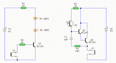
A Basic IR Link

Description:
A basic Imfra Red Link for audio communication for distances upto 3 metres.


Notes:
Ovo je shema jednostavne bez?i?ne komunikacije sa malo komponenata .Diode d1 i d2 su infracrvene le-diode ,a foto transistor je tako?er infracrveni radi ?to manjeg vanjskog utjecaja .Domet ure?aja je oko 3m no on se mo?e promijeniti brojem le-dioda i naponom koji se dovede na diode.Na izlaz se ?ak mogu i direktno spojiti slu?alice.Link mo?e poslu?iti i za prijenos drugih vrsta signala..Na popisu komponenata nema kriti?nih dijelova i izrada sklopa je jako jeftina. Uz malo pa?nje ne moe da ne radi.
P.S Transistors can be replaced with 2N3904 and 2N2222

Notes:
In his circuit Milan has created a basic Infra Red transmitter and receiver. The transmitter comprises a single amplifying stage driving two series connected IR LEDS. The input source is connected to J1. Please note that the device will pass a small DC current through it and also directly bias the transistor. A suitable device is therefore a high output crystal microphone. These can produce high output voltages up to 1 Volt but this will be reduced by the transistors low input impedance.

The receiver is three stages, the first stage being a phototransistor. Stages two and three form a high gain darlington emitter follower, the bias for the whole stage derived through R2 and the phototransistor itself. C1 and R3 form a filter to reduce interference from flourescent lighting and other hum sources. The output is via Jack J2. Note also that the output device will pass a small DC current so a medium impedance loudspeaker or hwadphones are a good choice here.
ReadMore..

Saturday, August 31, 2013

2 Channel Audio Mixer Using by Transistors

This 2 channels audio mixer is based on the 2n3904 transistors which forms 2 preamplifiers. The first preamplifier of the audio mixer has a high gain and can be used for microphone input, and the second one can be used to control the input of the audio level.

2 Channel Audio Mixer Circuit diagram


This two channel audio mixer require a power supply with the output voltage between 9 to 12 volts . For the audio signal you can use a CD player, mp3 player or other audio device and for the microphone you can use a normal dynamic microphone .

ReadMore..

Friday, August 16, 2013

Four Stage FM Transmitter

This FM transmitter circuit uses four radio frequency stages: a VHF oscillator built around transistor BF494 (T1), a preamplifier built around transistor BF200 (T2), a driver built around transistor 2N2219 (T3) and a power amplifier built around transistor 2N3866 (T4). A condenser microphone is connected at the input of the oscillator.

Working of the circuit is simple. When you speak near the microphone, frequency-modulated signals are obtained at the collector of oscillator transistor T1. The FM signals are amplified by the VHF preamplifier and the pre-driver stage. You can also use transistor 2N5109 in place of 2N2219. The preamplifier is a tuned class-A RF amplifier and the driver is a class-C amplifier. Signals are finally fed to the class-C RF power amplifier, which delivers RF power to a 50-ohm horizontal dipole or ground plane antenna. Use a heat-sink with transistor 2N3866 for heat dissipation. Carefully adjust trimmer VC1 connected across L1 to generate frequency within 88-108 MHz. Also adjust trimmers VC2 through VC7 to get maximum output at maximum range.

image Four Stage FM Transmitter circuit diagram
Regulator IC 78C09 provides stable 9V supply to the oscillator, so variation in the supply voltage will not affect the frequency generated. You can also use a 12V battery to power the circuit. Assemble the circuit on a general-purpose PCB. Install the antenna properly for maximum range. Coils L1 through L5 are made with 20 SWG copper-enamelled wire wound over air-cores having 8mm diameter. They have 4, 6, 6, 5 and 7 turns of wire, respectively.

EFY note. This transmitter is meant only for educational purposes. use of this transmitter with outdoor antenna is illegal in most parts of the world. The author and EFY will not be responsible for any misuse of this transmitter.

Copyright: EFY Mag
ReadMore..

Thursday, August 15, 2013

DTMF Proximity Detector

A DTMF-based IR transmitter and receiver pair can be used to realize a proximity detector. The circuit presented here enables you to detect any object capable of reflecting the IR beam and moving in front of the IR LED photo-detector pair up to a distance of about 12 cm from it. The circuit uses the commonly available telephony ICs such as dial-tone generator 91214B/91215B (IC1) and DTMF decoder CM8870 (IC2) in conjunction with infrared LED (IR LED1), photodiode D1, and other components as shown in the figure. A properly regulated 5V DC power supply is required for operation of the circuit.

The transmitter part is configured around dialer IC1. Its row 1 (pin 15) and column 1 (pin 12) get connected together via transistor T2 after a power-on delay (determined by capacitor C1 and resistors R1 and R16 in the base circuit of the transistor) to generate DTMF tone (combination of 697 Hz and 1209 Hz) corresponding to keypad digit “1” continuously. LED 2 is used to indicate the tone output from IC3. This tone output is amplified by Darlington transistor pair of T3 and T4 to drive IR LED1 via variable resistor VR1 in series with fixed 10-ohm resistor R14. Thus IR LED1 produces tone-modulated IR light.

DTMF Proximity Detector circuit diagramVariable resistor VR1 controls the emission level to vary the transmission range. LED 3 indicates that transmission is taking place. A part of modulated IR light signal transmitted by IR LED1, after reflection from an object, falls on photodetector diode D1. (The photodetector is to be shielded from direct IR light transmission path of IR LED1 by using any opaque partition so that it receives only the reflected IR light.) On detection of the signal by photodetector, it is coupled to DTMF decoder IC2 through emitter-follower transistor T1.

When the valid tone pair is detected by the decoder, its StD pin 15 (shorted to TOE pin 10) goes ‘high’. The detection of the object in proximity of IR transmitter-receiver combination is indicated by LED1. The active-high logic output pulse (terminated at connector CON1, in the figure) can be used to switch on/off any device (such as a siren via a latch and relay driver) or it can be used to clock a counter, etc. This DTMF proximity detector finds applications in burglar alarms, object counter and tachometers, etc.
 
 
Sourced by : Streampowers
ReadMore..