Saturday, August 31, 2013

2 Channel Audio Mixer Using by Transistors

This 2 channels audio mixer is based on the 2n3904 transistors which forms 2 preamplifiers. The first preamplifier of the audio mixer has a high gain and can be used for microphone input, and the second one can be used to control the input of the audio level.

2 Channel Audio Mixer Circuit diagram


This two channel audio mixer require a power supply with the output voltage between 9 to 12 volts . For the audio signal you can use a CD player, mp3 player or other audio device and for the microphone you can use a normal dynamic microphone .

ReadMore..

Friday, August 16, 2013

Four Stage FM Transmitter

This FM transmitter circuit uses four radio frequency stages: a VHF oscillator built around transistor BF494 (T1), a preamplifier built around transistor BF200 (T2), a driver built around transistor 2N2219 (T3) and a power amplifier built around transistor 2N3866 (T4). A condenser microphone is connected at the input of the oscillator.

Working of the circuit is simple. When you speak near the microphone, frequency-modulated signals are obtained at the collector of oscillator transistor T1. The FM signals are amplified by the VHF preamplifier and the pre-driver stage. You can also use transistor 2N5109 in place of 2N2219. The preamplifier is a tuned class-A RF amplifier and the driver is a class-C amplifier. Signals are finally fed to the class-C RF power amplifier, which delivers RF power to a 50-ohm horizontal dipole or ground plane antenna. Use a heat-sink with transistor 2N3866 for heat dissipation. Carefully adjust trimmer VC1 connected across L1 to generate frequency within 88-108 MHz. Also adjust trimmers VC2 through VC7 to get maximum output at maximum range.

image Four Stage FM Transmitter circuit diagram
Regulator IC 78C09 provides stable 9V supply to the oscillator, so variation in the supply voltage will not affect the frequency generated. You can also use a 12V battery to power the circuit. Assemble the circuit on a general-purpose PCB. Install the antenna properly for maximum range. Coils L1 through L5 are made with 20 SWG copper-enamelled wire wound over air-cores having 8mm diameter. They have 4, 6, 6, 5 and 7 turns of wire, respectively.

EFY note. This transmitter is meant only for educational purposes. use of this transmitter with outdoor antenna is illegal in most parts of the world. The author and EFY will not be responsible for any misuse of this transmitter.

Copyright: EFY Mag
ReadMore..

Thursday, August 15, 2013

DTMF Proximity Detector

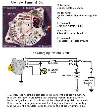
A DTMF-based IR transmitter and receiver pair can be used to realize a proximity detector. The circuit presented here enables you to detect any object capable of reflecting the IR beam and moving in front of the IR LED photo-detector pair up to a distance of about 12 cm from it. The circuit uses the commonly available telephony ICs such as dial-tone generator 91214B/91215B (IC1) and DTMF decoder CM8870 (IC2) in conjunction with infrared LED (IR LED1), photodiode D1, and other components as shown in the figure. A properly regulated 5V DC power supply is required for operation of the circuit.

The transmitter part is configured around dialer IC1. Its row 1 (pin 15) and column 1 (pin 12) get connected together via transistor T2 after a power-on delay (determined by capacitor C1 and resistors R1 and R16 in the base circuit of the transistor) to generate DTMF tone (combination of 697 Hz and 1209 Hz) corresponding to keypad digit “1” continuously. LED 2 is used to indicate the tone output from IC3. This tone output is amplified by Darlington transistor pair of T3 and T4 to drive IR LED1 via variable resistor VR1 in series with fixed 10-ohm resistor R14. Thus IR LED1 produces tone-modulated IR light.

DTMF Proximity Detector circuit diagramVariable resistor VR1 controls the emission level to vary the transmission range. LED 3 indicates that transmission is taking place. A part of modulated IR light signal transmitted by IR LED1, after reflection from an object, falls on photodetector diode D1. (The photodetector is to be shielded from direct IR light transmission path of IR LED1 by using any opaque partition so that it receives only the reflected IR light.) On detection of the signal by photodetector, it is coupled to DTMF decoder IC2 through emitter-follower transistor T1.

When the valid tone pair is detected by the decoder, its StD pin 15 (shorted to TOE pin 10) goes ‘high’. The detection of the object in proximity of IR transmitter-receiver combination is indicated by LED1. The active-high logic output pulse (terminated at connector CON1, in the figure) can be used to switch on/off any device (such as a siren via a latch and relay driver) or it can be used to clock a counter, etc. This DTMF proximity detector finds applications in burglar alarms, object counter and tachometers, etc.
 
 
Sourced by : Streampowers
ReadMore..

Wednesday, August 14, 2013

Christmas star with 40 LEDs

This is an ordinary LED circuit.Here you must be creative when you build this circuit.Really If you are creative you can make really really fantastic Christmas star.On the other hand you can use this for your Christmas tree even.


Note

# Use 6v for this circuit
# Use blue colour LEDs to get the maximum attraction.
ReadMore..

Tuesday, August 13, 2013

Thermostat Wiring Conventional Furnace Conditioner Split

Thermostat Wiring Diagram on Water Heater Typical Electric Water Heater Construction Wiring Diagram
Water Heater Typical Electric Water Heater Construction Wiring Diagram.


Thermostat Wiring Diagram on Wiring And Connectors Locations Of Honda Accord Air Conditioning
Wiring And Connectors Locations Of Honda Accord Air Conditioning.


Thermostat Wiring Diagram on Diagram Complete With Its Related Parts And Components Assembly
Diagram Complete With Its Related Parts And Components Assembly.


Thermostat Wiring Diagram on Schematic Diagram For Electronic Thermostat Of Isuzu Trooper Air
Schematic Diagram For Electronic Thermostat Of Isuzu Trooper Air.


Thermostat Wiring Diagram on Thermostat Wiring For Conventional Gas Furnace Air Conditioner Split
Thermostat Wiring For Conventional Gas Furnace Air Conditioner Split.


Thermostat Wiring Diagram on Sanyo Air Conditioners And Heat Pump Electrical Wiring Diagram
Sanyo Air Conditioners And Heat Pump Electrical Wiring Diagram.


Thermostat Wiring Diagram on About 1997 Chevrolet Venture Charging Circuit And Wiring Diagram
About 1997 Chevrolet Venture Charging Circuit And Wiring Diagram.


Thermostat Wiring Diagram on The Following Electrical Wiring Diagram Manual Apply For 1996 Mazda
The Following Electrical Wiring Diagram Manual Apply For 1996 Mazda.


Thermostat Wiring Diagram on Digital Thermostat Hunter Wiring Diagram 1 Jpg
Digital Thermostat Hunter Wiring Diagram 1 Jpg.


Thermostat Wiring Diagram on Wiring Diagram Of Nuheat Solo Programmable Thermostat   Around
Wiring Diagram Of Nuheat Solo Programmable Thermostat Around.


ReadMore..

Monday, August 12, 2013

Drinking Water Alarm

Drinking Water Alarm

The
State Jal Boards supply water for limited duration in a day. Time of
water supply is decided by the management and the public does not know
the same. In such a situation, this water alarm circuit will save the
people from long wait as it will inform them as soon as the water supply
starts. At the heart of this circuit is a small water sensor. For
fabricating this water sensor, you need two foils—an aluminium foil and a
plastic foil. You can assemble the sensor by rolling aluminium and
plastic foils in the shape of a concentric cylinder. Connect one end of
the insulated flexible wire on the aluminium foil and the other end to
resistor R2. Now mount this sensor inside the water tap such that water
can flow through it uninterrupted. To complete the circuit, connect
another wire from the junction of pins 2 and 6 of IC1 to the water
pipeline or the water tap itself. The working of the circuit is simple.

Drinking Water alarm Circuit DiagramTimer
555 is wired as an astable multivibrator. The multivibrator will work
only when water flows through the water tap and completes the circuit
connection. It oscillates at about 1 kHz. The output of the timer at pin
3 is connected to loudspeaker LS1 via capacitor C3. As soon as water
starts flowing through the tap, the speaker starts sounding, which
indicates resumption of water supply. It remains ‘on’ until you switch
off the circuit with switch S1 or remove the sensor from the tap. The
circuit works off a 9V battery supply. Assemble the circuit on any
general-purpose PCB and house in a suitable cabinet. The water sensor is
inserted into the water tap. Connect the lead coming out from the
junction of 555 pins 2 and 6 to the body of the water tap. Use on/off
switch S1 to power the circuit with the 9V PP3 battery.
ReadMore..

Sunday, August 11, 2013

Very Low Power 32kHz Oscillator

The 32-kHz low-power clock oscillator offers numerous advantages over conventional oscillator circuits based on a CMOS inverter. Such inverter circuits present problems, for example, supply currents fluctuate widely over a 3V to 6V supply range, while current consumption below 250 µA is difficult to attain. Also, operation can be unreliable with wide variations in the supply voltage and the inverter’s input characteristics are subject to wide tolerances and differences among manufacturers. The circuit shown here solves the above problems. Drawing just 13 µA from a 3V supply, it consists of a one-transistor amplifier/oscillator (T1) and a low-power comparator/reference device (IC1).

Circuit diagram:
very-low-power-32khz-oscillator-circuit-diagram Very Low Power 32kHz Oscillator Circuit Diagram

The base of T1 is biased at 1.25 V using R5/R4 and the reference in IC1. T1 may be any small-signal transistor with a decent beta of 100 or so at 5 µA (defined here by R3, fixing the collector voltage at about 1 V below Vcc). The amplifier’s nominal gain is approximately 2 V/V. The quartz crystal combined with load capacitors C1 and C3 forms a feedback path around T1, whose 180 degrees of phase shift causes the oscillation. The bias voltage of 1.25 V for the comparator inside the MAX931 is defined by the reference via R2. The comparator’s input swing is thus accurately centred around the reference voltage.

Operating at 3 V and 32 kHz, IC1 draws just 7 µA. The comparator output can source and sink 40 mA and 5 mA respectively, which is ample for most low-power loads. However, the moderate rise/fall times of 500 ns and 100 ns respectively can cause standard, high-speed CMOS logic to draw higher than usual switching currents. The optional 74HC14 Schmitt trigger shown at the circuit output can handle the comparator’s rise/fall times with only a small penalty in supply current.


Source by : Streampowers
ReadMore..

Saturday, August 10, 2013

Simple Light Dependent Resistors

LDRs or lightweight Dependent Resistors are terribly helpful particularly in light/dark sensor circuits. Normally the resistance of an LDR is incredibly high, typically as high as a thousand 000 ohms, however once they are illuminated with lightweight resistance drops dramatically.


 The animation opposite shows that when the torch is turned on, the resistance of the LDR falls, permitting current to have it.Circuit Wizard software has been used to show, the vary of values of a ORP12, LDR .
When a light-weight level of a thousand lux (bright light) is directed towards it, the resistance is 400R (ohms).


When a light-weight level of ten lux (very low light level) is directed towards it, the resistance has risen dramatically to ten.43M (10430000 ohms).

This is an example of a light-weight sensor circuit :

When the sunshine level is low the resistance of the LDR is high. This prevents current from flowing to the bottom of the transistors. Consequently the LED doesnt lightweight. However, when lightweight shines onto the LDR its resistance falls and current flows into the bottom of the primary transistor and then the second transistor. The LED lights.

The preset resistor will be turned up or right down to increase or decrease resistance, during this means it will build the circuit additional or less sensitive. Link

ReadMore..

Friday, August 9, 2013

Battery Powered Night Lamp

This circuit is usable as a Night Lamp when a wall mains socket is not available to plug-in an ever running small neon lamp device. In order to ensure minimum battery consumption, one 1.5V cell is used and simple voltage doublers drives a pulsating ultra-bright LED: current drawing is less than 500µA. An optional Photo resistor will switch-off the circuit in daylight or when room lamps illuminate, allowing further current economy. This device will run for about 3 months continuously on an ordinary AA sized cell or for around 6 months on an alkaline type cell but, adding the Photo resistor circuitry, running time will be doubled or, very likely, triplicates. IC1 generates a square wave at about 4 Hz frequencies. C2 & D2 form voltage doublers, necessary to raise the battery voltage to a peak value able to drive the LED.


Parts:

R1 = 1M
R2 = 1M
R3 = 47K
R4 = LDR
C1 = 100nF-63V
C2 = 220uF-25V
D1 = Ultra Bright 10mm LED
D2 = 1N5819 B1 = 1.5V Battery or AA Cell
IC1 = 7555 CMos Timer IC

Notes:
* IC1 must be a CMos type: only these devices can safely operate at 1.5V supply or less. * If you do not need Photo resistor operation, omit R3 & R4 and connect pin 4 of IC1 to positive supply. * Ordinary LEDs can be used, but light intensity will be poor. * An ordinary 1N4148 type diode can be used instead of the 1N5819 Schottky-barrier type diode, but LED intensity will be reduced due to the higher voltage drop. * Any Schottky-barrier type diode can be used in place of the 1N5819, e.g. the BAT46, rated @ 100V 150mA.
ReadMore..

Thursday, August 8, 2013

Simple Automatic Switch For Audio Power Amplifier

Circuit of an automatic switch for audio power amplifier stage is presented here. The circuit uses stereo preamplifier output to detect the presence of audio to switch the audio power amplifier on only when audio is present. The circuit thus helps curtail power wastage. IC1 is used as an inverting adder. The input signals from left and right channels are combined to form a common signal for IC2, which is used as an open loop comparator. IC3 (NE556) is a dual timer. Its second section, i.e., IC3(b), is configured as monostable multivibrator. Output of IC3(b) is used to switch the power amplifier on or off through a Darlington pair formed by transistors T1 and T2. IC3(a) is used to trigger the monostable multivibrator whenever an input signal is sensed.

Circuit diagram:
Automatic Switch For Audio Power Amplifier-Circuit-Diagram
Automatic Switch For Audio Power Amplifier Circuit Diagram

Under ‘no signal’ condition, pin 3 of IC2 is negative with respect to its pin 2. Hence the output of IC2 is low and as a result output of IC3(a) is high. Since there is no trigger at pin 8 of IC3(b), the output of IC3(b) will be low and the amplifier will be off. When an input singal is applied to IC1, IC2 converts the inverted sum of the input signals into a rectangular waveform by comparing it with a constant voltage which can be controlled by varying potentiometer VR1. When the output of IC2 is high, output pin 5 of IC3 goes low, thus triggering the monostable multivibrator. As soon as the audio input to IC1 stops, pin 5 of IC3 goes high and pin 1 of IC3 discharges through capacitor C3, thus resetting the monostable multivibrator. 

Hence, as long as input signals are applied, the amplifier remains ‘on.’ When the input signals are removed, i.e., when signal level is zero, the amplifier switches off after the mono flip-flop delay period determined by the values of resistor R8 and capacitor C3. If no input signals are sensed within this time, the amplifier turns off—else it remains on. Power supply for the circuit can be obtained from the power supply of the amplifier. Hence, the circuit can be permanently fitted in the amplifier box itself. The main switch of the amplifier should be always kept on. Resistors R1 and R2 are used to divide single voltage supply into two equal parts.

Capacitors C1 and C2 are used as regulators and also as an AC bypass for input signals. Diode D1 is used so that loading fluctuations in power amplifier do not affect circuit regulation. Transisitor T2 acts as a high voltage switch which may be replaced by any other high voltage switching transistor satisfying amplifier current requirements. Value of resistor R10 should be modified for large current requirement. The LED glows when the amplifier is on. The circuit is very useful and relieves one from putting the amplifier on and off every time one plays a cassette or radio etc.


http://streampowers.blogspot.com/2012/06/simple-automatic-switch-for-audio-power_11.html
ReadMore..

Wednesday, August 7, 2013

Soft Start For Switching Power Supply


Switching power supply whose output voltage is appreciably lower than its input voltage has an interesting property: the current drawn by it is smaller than its output current. However, the input power (UI) is, of course, greater than the output power. There is another aspect that needs to be watched: when the input voltage at switch-on is too low, the regulator will tend to draw the full current. When the supply cannot cope with this, it fails or the fuse blows. It is, therefore, advisable to disable the regulator at switch-on (via the on/off input). until the relevant capacitor has been charged. When the regulator then starts to draw current, the charging current has already dropped to a level which does not overload the voltage source.

Circuit diagram:
 Soft Start Circuit Diagram For Switching Power Supply
Soft Start Circuit For Switching Power Supply

The circuit in the diagram provides an output voltage of 5 V and is supplied by a 24 V source. The regulator need not be disabled until the capacitor is fully charged: when the potential across the capacitor has reached a level of half or more of the input voltage, all is well. This is why the zener diode in the diagram is rated at 15 V. Many regulators produced by National Semiconductor have an integral on/off switch, and this is used in the present circuit. The input is intended for TTL signals, and usually consists of a transistor whose base is accessible externally. This means that a higher switching voltage may be applied via a series resistor: the value of this in the present circuit is 22 kΩ. When the voltage across the capacitor reaches a level of about 17 V, transistor T1 comes on, whereupon the regulator is enabled.
Source: National Semiconductors
ReadMore..

Tuesday, August 6, 2013

Alternator Wiring Diagrams

Alternator Wiring Diagram on Wiring 12v Marine Tachometer Diesel Alternator Instructions   How To
Wiring 12v Marine Tachometer Diesel Alternator Instructions How To.


Alternator Wiring Diagram on Delco One Wire Alternator Installation On 5000 Ford Mf135 Wiring Rjs
Delco One Wire Alternator Installation On 5000 Ford Mf135 Wiring Rjs.


Alternator Wiring Diagram on Here S A Wiring Diagram For The Denso Alternator
Here S A Wiring Diagram For The Denso Alternator.


Alternator Wiring Diagram on Typical Alternator Wiring Diagram An Alternator Is A Three
Typical Alternator Wiring Diagram An Alternator Is A Three.


Alternator Wiring Diagram on Westfield World Kitcar Support Site   Wiring A Nippon Denso Alternator
Westfield World Kitcar Support Site Wiring A Nippon Denso Alternator.


Alternator Wiring Diagram on Thread  Auto  Leco S   Help With Some Alternator Wiring Please
Thread Auto Leco S Help With Some Alternator Wiring Please.


Alternator Wiring Diagram on Suggested Wiring Diagram For Alternator Field Disconnect Circuit
Suggested Wiring Diagram For Alternator Field Disconnect Circuit.


Alternator Wiring Diagram on Gm 3 Wire Alternator Idiot Light Hook Up   Hot Rod Forum   Hotrodders
Gm 3 Wire Alternator Idiot Light Hook Up Hot Rod Forum Hotrodders.


Alternator Wiring Diagram on Serpentine Alternator Wiring
Serpentine Alternator Wiring.


Alternator Wiring Diagram on Alternator Wiring Diagrams  1g  2g  And 3g
Alternator Wiring Diagrams 1g 2g And 3g.


ReadMore..

Monday, August 5, 2013

Overload Speaker Protection Circuit Diagram

Overload Speaker Protection Circuit Diagram input is taken from the terminal loudspeaker or amplifier output jacks. If the right channel is large enough to charge C1 to a potential which exceeds the breakdown voltage of the emitter of Ql, a voltage pulse appears in R7. Similarly, if the left channel signal is large enough to charge C2 to a voltage that is greater than the breakdown voltage of the emitter of Q2 `, a pulse appears in R7. The pulse triggers in R7 5CRI. A door sensitive SCR (LGT less than 15 RNA or IGT is the gate-trigger current) that locks in a conducting state and energizes Ryl. The action of the relay will interrupt the speaker circuit. and silence follows you must alert on the problem. 

 Overload Speaker Protection Circuit Diagram

Overload Speaker Protection Circuit Diagram


Reduce the volume on your amplifier, then press and release 51 to reset the circuit and restore normal operation. The circuit can be set to go off at any level of 15 watts RMS to 150. To calibrate . deliberately over-power signal at the entrance of the right speaker protection and adjust R3 until RY1 boosts. Do the same with the left channel, this time adjusting R4. The circuit is now calibrated and ready employment.
ReadMore..

Sunday, August 4, 2013

Build a LT3582 12 DC 5V to 12V DC Converter

Using LT3582-12 dual channel DC DC converter integrated circuit, manufactured by Linear Technology, can be designed a very simple step up dc converter. This 5 to 12V c converter electronic project provide both positive and negative outputs required in many biasing applications such as active matrix OLED (organic light-emitting diode)displays as well as CCD (charge coupled device) applications.

Build a LT3582-12 DC 5V to 12V DC Converter

The LT3582 offer an I2C interface that can dynamically program output voltages, power sequencing and output voltage ramps as the application requires. The LT3582’s positive output voltage can be set between 3.2V and 12.775 in 25mV steps, whereas the negative output can be set between -1.2V and -13.95V in 50mV steps. The LT3582-12 is preconfigured with ±12V output, requiring no future programming.
ReadMore..

Saturday, August 3, 2013

MOUSE REPELLENT ELECTRONIC CIRCUIT DIAGRAM

MOUSE REPELLENT ELECTRONIC CIRCUIT DIAGRAM

When the circuit at its close state, the IC will control the buzzer time using the resistor and capacitor. The buzzer sounds like alarm in the different frequencies.

  •     Resistor R1 : 1.8k ohm
  •     Resistor R2 : 1k ohm
  •     Resistor R3 : 5.6k ohm
  •     Resistor R4 : 480 ohm
  •     Capacitor C1 : 2.2 nF
  •     Polar Capacitor C2 : 0.022uF/6V
  •     IC1 timer : NE555
  •     Speaker SP1 : Tweeter 8 ohm
  •     Power supply : 5V
ReadMore..

Friday, August 2, 2013

Frequency Tone Decoder Circuit Using TC9400 FVC

Another application of FVC (frequency-to-voltage converter) is tone/frequency decoder. This circuit is used to determine the frequency band of an oscillation signal. This circuit is used in many application like determines the frequency band in the signal and remote control where the frequency band corresponds to a different command. This circuit uses TC9400 F/V converter to convert the frequency to voltage because the frequency must be converted to proportional analog voltage before can be detected. This is the figure of the circuit;


Beside TC9400 F/V converter, this circuit also uses the quad comparators. It used to detect when the frequency limits is exceeded by the voltage (frequency). The frequency is indicated by the logical “1″ at any of the five output. [Circuit diagram source: Microchip Application Note]
ReadMore..

Thursday, August 1, 2013

9V FM Transmitter

This fm transmitter circuit is a very simple and require few external components and operates in FM band above 100 MHz.This fm transmitter needs to be powered from a 9 volts battery or from another 9 volts regulated power supply .The tuned coil L1, has two output tapping for the antenna connection, marked "A" and "B".

These are both low-level outputs and you choose which tapping you want to use ( stable low range, or more unstable but higher range). Tap B (2.5%) takes just a very small portion of signal from the oscillator circuit and therefore gives a very frequency stable transmitter. The output level (around 2.5mW) and range are therefore somewhat reduced.Tap A (10%) delivers very much more power (around 10mW) to the antenna load. This gives you a greater range, but at the expense of frequency stability. 

9V FM Transmitter Circuit diagram


All component leads should be kept as short as possible. The LINK wire on the PCB should lay flat on the PCB. Use the cutoff from a resistor leg.  Antenna length for circuit diagram transmitter varies with frequency for optimum distance: 90MHz 80 cm, 95MHz 75cm, 100MHz 70 cm, 105 MHz 68 cm.The frequency determining elements (L1, C5 and C6) form a simple LC tuned oscillator. The inherent problem with this type of circuit diagram transmitter is that any external load (antenna) will change the operating frequency.
ReadMore..