Wednesday, August 7, 2013
Soft Start For Switching Power Supply
Switching power supply whose output voltage is appreciably lower than its input voltage has an interesting property: the current drawn by it is smaller than its output current. However, the input power (UI) is, of course, greater than the output power. There is another aspect that needs to be watched: when the input voltage at switch-on is too low, the regulator will tend to draw the full current. When the supply cannot cope with this, it fails or the fuse blows. It is, therefore, advisable to disable the regulator at switch-on (via the on/off input). until the relevant capacitor has been charged. When the regulator then starts to draw current, the charging current has already dropped to a level which does not overload the voltage source.
Circuit diagram:

Circuit diagram:
Soft Start Circuit For Switching Power Supply
The circuit in the diagram provides an output voltage of 5 V and is supplied by a 24 V source. The regulator need not be disabled until the capacitor is fully charged: when the potential across the capacitor has reached a level of half or more of the input voltage, all is well. This is why the zener diode in the diagram is rated at 15 V. Many regulators produced by National Semiconductor have an integral on/off switch, and this is used in the present circuit. The input is intended for TTL signals, and usually consists of a transistor whose base is accessible externally. This means that a higher switching voltage may be applied via a series resistor: the value of this in the present circuit is 22 kΩ. When the voltage across the capacitor reaches a level of about 17 V, transistor T1 comes on, whereupon the regulator is enabled.
Source: National Semiconductors

Tuesday, August 6, 2013
Alternator Wiring Diagrams

Wiring 12v Marine Tachometer Diesel Alternator Instructions How To.

Delco One Wire Alternator Installation On 5000 Ford Mf135 Wiring Rjs.
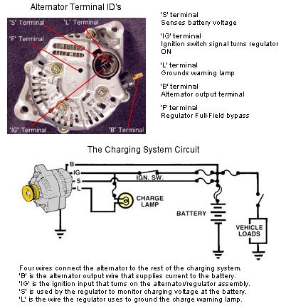
Here S A Wiring Diagram For The Denso Alternator.

Typical Alternator Wiring Diagram An Alternator Is A Three.
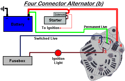
Westfield World Kitcar Support Site Wiring A Nippon Denso Alternator.
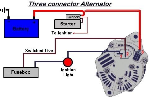
Thread Auto Leco S Help With Some Alternator Wiring Please.

Suggested Wiring Diagram For Alternator Field Disconnect Circuit.
Gm 3 Wire Alternator Idiot Light Hook Up Hot Rod Forum Hotrodders.
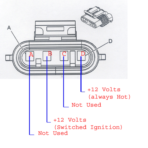
Serpentine Alternator Wiring.
Alternator Wiring Diagrams 1g 2g And 3g.
Monday, August 5, 2013
Overload Speaker Protection Circuit Diagram
Overload Speaker Protection Circuit Diagram input is taken from the terminal loudspeaker or amplifier output jacks. If the right channel is large enough to charge C1 to a potential which exceeds the breakdown voltage of the emitter of Ql, a voltage pulse appears in R7. Similarly, if the left channel signal is large enough to charge C2 to a voltage that is greater than the breakdown voltage of the emitter of Q2 `, a pulse appears in R7. The pulse triggers in R7 5CRI. A door sensitive SCR (LGT less than 15 RNA or IGT is the gate-trigger current) that locks in a conducting state and energizes Ryl. The action of the relay will interrupt the speaker circuit. and silence follows you must alert on the problem.
Overload Speaker Protection Circuit Diagram

Reduce the volume on your amplifier, then press and release 51 to reset the circuit and restore normal operation. The circuit can be set to go off at any level of 15 watts RMS to 150. To calibrate . deliberately over-power signal at the entrance of the right speaker protection and adjust R3 until RY1 boosts. Do the same with the left channel, this time adjusting R4. The circuit is now calibrated and ready employment.
Sunday, August 4, 2013
Build a LT3582 12 DC 5V to 12V DC Converter
Using LT3582-12 dual channel DC DC converter integrated circuit, manufactured by Linear Technology, can be designed a very simple step up dc converter. This 5 to 12V c converter electronic project provide both positive and negative outputs required in many biasing applications such as active matrix OLED (organic light-emitting diode)displays as well as CCD (charge coupled device) applications.

The LT3582 offer an I2C interface that can dynamically program output voltages, power sequencing and output voltage ramps as the application requires. The LT3582’s positive output voltage can be set between 3.2V and 12.775 in 25mV steps, whereas the negative output can be set between -1.2V and -13.95V in 50mV steps. The LT3582-12 is preconfigured with ±12V output, requiring no future programming.
Saturday, August 3, 2013
MOUSE REPELLENT ELECTRONIC CIRCUIT DIAGRAM

MOUSE REPELLENT ELECTRONIC CIRCUIT DIAGRAM
When the circuit at its close state, the IC will control the buzzer time using the resistor and capacitor. The buzzer sounds like alarm in the different frequencies.
- Resistor R1 : 1.8k ohm
- Resistor R2 : 1k ohm
- Resistor R3 : 5.6k ohm
- Resistor R4 : 480 ohm
- Capacitor C1 : 2.2 nF
- Polar Capacitor C2 : 0.022uF/6V
- IC1 timer : NE555
- Speaker SP1 : Tweeter 8 ohm
- Power supply : 5V
Friday, August 2, 2013
Frequency Tone Decoder Circuit Using TC9400 FVC
Another application of FVC (frequency-to-voltage converter) is tone/frequency decoder. This circuit is used to determine the frequency band of an oscillation signal. This circuit is used in many application like determines the frequency band in the signal and remote control where the frequency band corresponds to a different command. This circuit uses TC9400 F/V converter to convert the frequency to voltage because the frequency must be converted to proportional analog voltage before can be detected. This is the figure of the circuit;

Beside TC9400 F/V converter, this circuit also uses the quad comparators. It used to detect when the frequency limits is exceeded by the voltage (frequency). The frequency is indicated by the logical “1″ at any of the five output. [Circuit diagram source: Microchip Application Note]
Thursday, August 1, 2013
9V FM Transmitter
This fm transmitter circuit is a very simple and require few external components and operates in FM band above 100 MHz.This fm transmitter needs to be powered from a 9 volts battery or from another 9 volts regulated power supply .The tuned coil L1, has two output tapping for the antenna connection, marked "A" and "B".
These are both low-level outputs and you choose which tapping you want to use ( stable low range, or more unstable but higher range). Tap B (2.5%) takes just a very small portion of signal from the oscillator circuit and therefore gives a very frequency stable transmitter. The output level (around 2.5mW) and range are therefore somewhat reduced.Tap A (10%) delivers very much more power (around 10mW) to the antenna load. This gives you a greater range, but at the expense of frequency stability.
9V FM Transmitter Circuit diagram

All component leads should be kept as short as possible. The LINK wire on the PCB should lay flat on the PCB. Use the cutoff from a resistor leg. Antenna length for circuit diagram transmitter varies with frequency for optimum distance: 90MHz 80 cm, 95MHz 75cm, 100MHz 70 cm, 105 MHz 68 cm.The frequency determining elements (L1, C5 and C6) form a simple LC tuned oscillator. The inherent problem with this type of circuit diagram transmitter is that any external load (antenna) will change the operating frequency.
These are both low-level outputs and you choose which tapping you want to use ( stable low range, or more unstable but higher range). Tap B (2.5%) takes just a very small portion of signal from the oscillator circuit and therefore gives a very frequency stable transmitter. The output level (around 2.5mW) and range are therefore somewhat reduced.Tap A (10%) delivers very much more power (around 10mW) to the antenna load. This gives you a greater range, but at the expense of frequency stability.
9V FM Transmitter Circuit diagram
All component leads should be kept as short as possible. The LINK wire on the PCB should lay flat on the PCB. Use the cutoff from a resistor leg. Antenna length for circuit diagram transmitter varies with frequency for optimum distance: 90MHz 80 cm, 95MHz 75cm, 100MHz 70 cm, 105 MHz 68 cm.The frequency determining elements (L1, C5 and C6) form a simple LC tuned oscillator. The inherent problem with this type of circuit diagram transmitter is that any external load (antenna) will change the operating frequency.
Subscribe to:
Posts (Atom)